LiNC80 SBC1 kits are available for purchase!
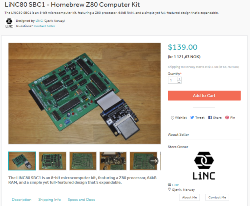
I am proud to announce that as of now, my LiNC80 SBC1 is available for purchase in kit form at Tindie!
It took me a few tries to get through the approval process, simply because the fairly high differences in the fairly high shipping costs incurred from using Posten Norge as my trusted carrier, forced me to make separate listings of Kit and PCB, and that caused issues, as Tindie weren't used to dealing with that.
I'm not sure if this is the culmination of or the start of a lot of hard work. Now starts the bit where I need to ship, restock, support and see what people make of it. But first of course the terrifying bit: will anyone actually purchase the kit?
If you want a compact, expandable, fun 8-bit retro computer reminiscent of 1979, head on over to my Tindie shop now!

Digital I/O card for my Z50Bus computer
While working towards getting my LiNC80 SBC1 kits ready for sale, I had a little bit of waiting-time to cover. During that time, Steve Cousins and I were talking about his boot-up status output using a standard I/O port, and that it would be nice if I would be able to provide a digital I/O card a short time after launching the kits.
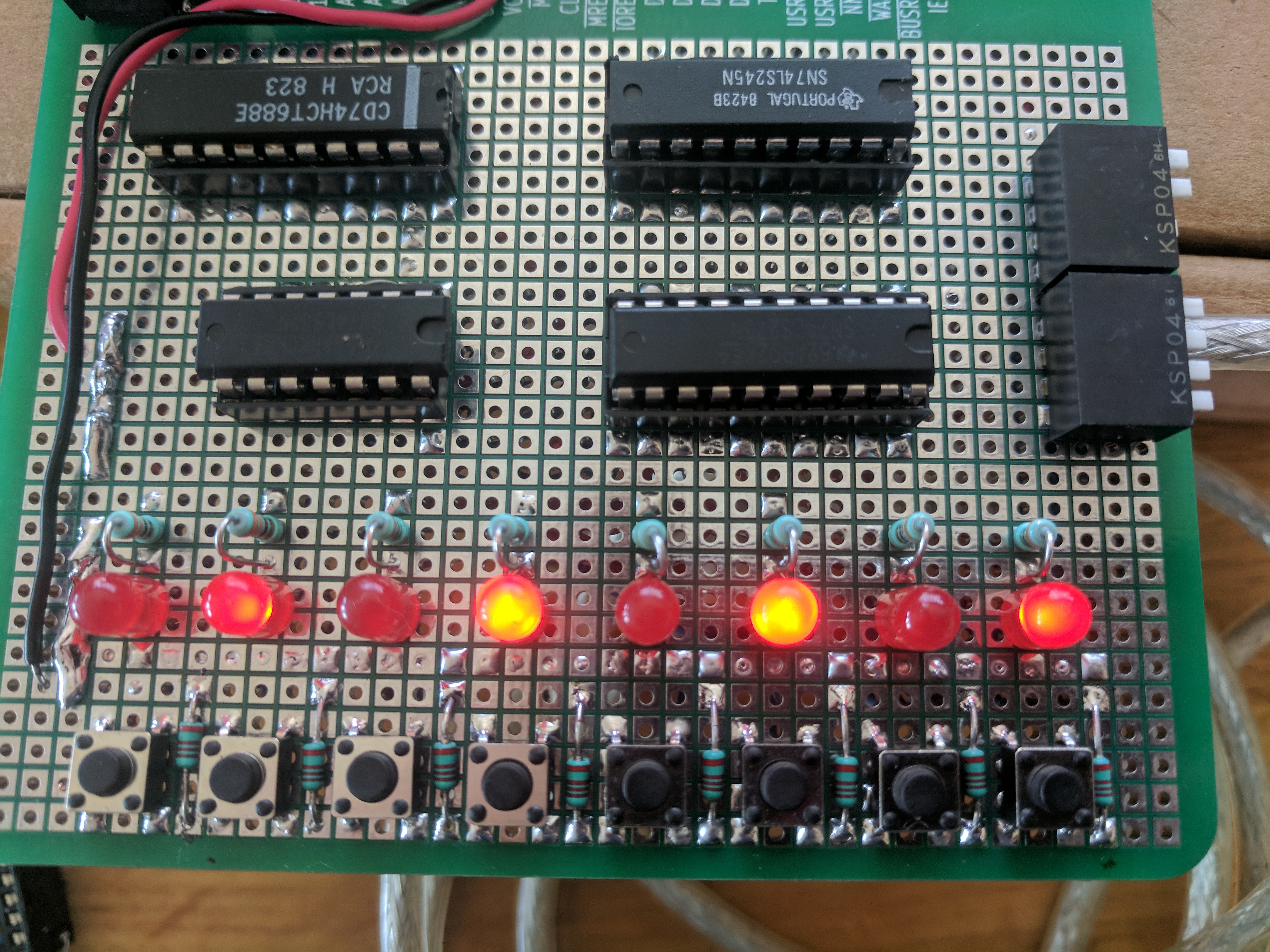
As I already had my prototype prototyping cards and a bit of time, I designed a card inspired by Spencer's RC2014 Digital I/O card, and assembled it using simple point-to-point wiring. As expected, the card performs exactly what it was designed to do, both when connected directly to the SBC and when connected to a 5-slot Z50Bus backplane.
This is a simple I/O card that uses a 74LS273 latch to receive and store output data displayed on eight LEDs, a 74LS245 bus tranceiver to "gate" the input switches/buttons as inputs, and a 74LS688 8-bit comparator to do full address decoding of 8 bits. The way the 8-bit comparator is used makes it possible for this card to use any single I/O address in the Z80 I/O address range. Writing to the selected address sets the output state, and reading the address reads the current values on the buttons/switches. Steve's SCMon uses the "reserved" address 0x30 as a simple output write port for status during boot, so setting this card's address to 0x30 allows the nice led-scroll to be seen 🙂
Based on the schematic below, I will start doing a PCB layout, and make this an official LiNC product as soon as the LiNC80 SBC1 launches proper.
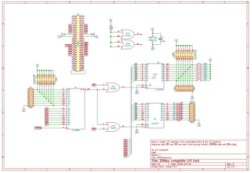
Z50IOCard schematic - click for full resolution PDF
Third-party software for a machine that’s not even shipping \o/
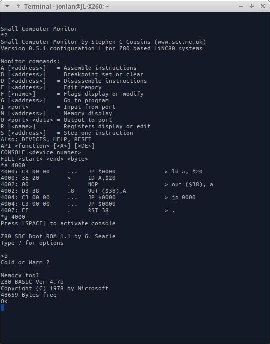
I mentioned in my previous post about the possibility for a ROM Monitor getting a port to my homebrew system. Yesterday, I received a mail, containing ASM-files and a compiled HEX file of the first attempt at a port. Even without access to hardware, Steve has been able to make a working version of SCMonitor for my system! It's still early, and uses RC2014/G.Searle style clocking of serial ports, but it boots and works!
Status of the LiNC80 SBC1 mid march 2018
Here's an update to those who are following my "homebrew" tag to see if I actually end up making kits available.
Kits are coming
I'm most definitely working to get kits of this microcomputer available. I have updated my company page over at linc.no/products, and that will be the "home" of the product side of things. I'm planning on selling the kits though Tindie when I get them, well, kitted up.
I've received permission from Grant Searle to include his software on ROM in the kits, and also his permission to make available changed code for the parts where I need to make changes. Getting his permission really made me happy. I've also been talking with Steve Cousins about the possibility of a future port of his Small Computer Monitor (SCMonitor), and we are both enthusiastic about that (scmonitor will not be included in kits, at least not at launch).
The base set of passive components, and the "jellybean parts" have all been ordered, or I already have them in stock. I've also done quite a bit of evaluations on materials needed for handling/packing/shipping, and there's a bunch of bags and boxes on their way to me currently.
Slight delay
I had hoped to have the kits available already, to be honest. Unfortunately that's obviously not the case. Brushing aside delays caused by funding, I've decided I need to halt the progress a bit. On the C-revision of the PCB, I have discovered that using only one Serial Port with the other not connected causes usability issues. When using SIOA, with nothing connected to SIOB, it's nearly impossible to get the computer to recognize the SPACE press needed at boot to select console. Also, when using only SIOB with nothing at SIOA, there's a case of character injection. Both of these are solved by simply adding two resistors on SIOA: a 470k pull-down on CTS, and a 470k pull-up on RX. I think the "I can't boot the computer" issue when using only SIOA is critical enough that I need to make a new revision of the PCB. This gives the option of fixing a few silk-screen errors, and adding a non-critical jumper to the board.
Before ordering new PCB's with the mentioned changes, I really want someone else besides me to actually try to build the kit. To get that accomplished, I've enlisted the help of a few friends who gets a kit each to build. Because I won't order new PCB's before I've had their feedback, I can't start making kits available before two weeks after they have built theirs.
Current schedule
Unless something else shows up along the way, I'm counting one week to get the "beta kits" out, two weeks for the "beta builders" to get their kits assembled, and another two weeks of assessments and finalization. That puts my "ready" date at the absolute end of April.
So if all goes according to plan, I should be able to have kits listed for sale with Tindie in the first week of may, with first possible deliveries the week after.
I have for some reason still not received any questions about prices, but I'll give an estimate. Looking over my numbers at the moment, it seems I need to charge somewhere close to US $160 for a kit, shipping not included. This is a rough number, and is likely to go down some, but not much. Currently mu shipping options is to use the Norwegian Post. They are quite expensive, but at least they are predictable: international letter (untracked) is ~US$18 flat rate, while tracked parcel is a whopping $49. EU addresses save a few € on each of those prices.
Playing with SunOS 4.1.4 SPARC on QEmu
I've previously tried getting SunOS 4 to run on the SPARC version of QEmu. Back then, my source of install media was a SunOS 4.1.2 CDROM that I had for my Sun SPARCstation IPC machines. Unfortunately, the only emulated old classic-style SPARCstation that I could get to even qemu-boot was the SPARCstation 5, and that hardware is not recognized by the Unix kernel on the CD, so it refuses to boot. The oldest version of SunOS4 that boots on the SS5 is SunOS 4.1.4, and I could not find install media for that version.
However, I recently realized that my quest for SunOS4 on QEmu could be completed! I had been stupid, and searched for install media for the wrong name! Sun decided to stop using the name SunOS when they started using more BSD/SysV mixing, and started using Solaris as the name instead. So, Solaris 1.1.2 is actually the name for SunOS 4.1.4! I managed to track down an ISO image that wanted to boot at https://winworldpc.com/product/sun-solaris/1x
Starting out with my old notes from a previous try at installing SunOS 4.1.2, I went with a 2GB QEmu disk image, as this matches nicely with a "type SUN2.1G" disk in the predefined disk layouts:
qemu-img create -f raw -o compat=1.1 sunos414.img 2G
Using that image, and the Solaris ISO file, I could start up QEmu (with an NVRAM clock set to before Y2K). Note that this is one command, I just split it across two lines here to make it readable.
qemu-system-sparc -vga cg3 -M SS-5 -bios ss5.bin -m 32
    -startdate "1999-04-19" -hda .\sunos414.img -hdb Solaris1_1_2.iso
Next, we need to boot the kernel that's in the D slice of the CDROM. If that doesn't make sense to you, that's perfectly OK. Sun installation CDROMs are actually UFS disk images with partitions, and UFS partitions have lettered labels. And in their wisdom, Sun placed the kernel on the fourth UFS partition (at least, that's how I understand it).
ok boot disk1:d
This boots the CDROM environment, starting the install process:
What would you like to do?
  1 - install SunOS mini-root
  2 - exit to single user shell
Enter a 1 or 2: 1
Beginning system installation - probing for disks.
Which disk do you want to be your miniroot system disk?
  1 - sd1:   at esp0 slave 8
  2 - sd3:  > at esp0 slave 0
  3 - exit to single user shell
Enter a 1, 2 or 3: 2
selected disk unit "sd3".
Do you want to format and/or label disk "sd3"?
  1 - yes, run format
  2 - no, continue with loading miniroot
  3 - no, exit to single user shell
Enter a 1, 2, or 3: 1
The format program on SunOS/Solaris isn't "format", but a combination of fdisk, format, and a bunch of other toools. Once it's started, we need to tell it what type of disk we have. With the 2GB QEmu image, the correct option is 13. If a different disk image size is used, it's probably possible to "make it supported" by fooling around with the configuration in /etc/format.dat. Good luck doing that on the CD.
format> type


AVAILABLE DRIVE TYPES:
        0. Quantum ProDrive 80S
        1. Quantum ProDrive 105S
        2. CDC Wren IV 94171-344
        3. SUN0104
        4. SUN0207
        5. SUN0320
        6. SUN0327
        7. SUN0424
        8. SUN0535
        9. SUN0669
        10. SUN1.0G
        11. SUN1.05
        12. SUN1.3G
        13. SUN2.1G
        14. CD-ROM Disc for SunOS Installation
        15. other
Specify disk type (enter its number): 13
selecting sd3:
[disk formatted, no defect list found]
format> label
Ready to label disk, continue? y

format> partition
partition> print
Current partition table (SUN2.1G_PREINSTALL):
        partition a - starting cyl      0, # blocks    62320 (41/0/0)
        partition b - starting cyl     41, # blocks   197600 (130/0/0)
        partition c - starting cyl      0, # blocks  4154160 (2733/0/0)
        partition d - starting cyl      0, # blocks        0 (0/0/0)
        partition e - starting cyl      0, # blocks        0 (0/0/0)
        partition f - starting cyl      0, # blocks        0 (0/0/0)
        partition g - starting cyl    171, # blocks  1947120 (1281/0/0)
        partition h - starting cyl   1452, # blocks  1947120 (1281/0/0)

partition> label
partition> quit
format> quit
checking writeability of /dev/rsd3b
0+1 records in
1+0 records out
Extracting miniroot ...
using cdrom partition number 3
fastread: failed to open /dev/rsr0No such device or address
ERROR while loading miniroot disk: /dev/rsd3b
And this is where I initially got stuck, and ended up at https://en.wikibooks.org/wiki/QEMU/SunOS_4.1.4.
The doc' there is so close to identical to what I've done so far, I suspect it's the guide I got my instructions for when I tried the older SunOS previously. Anywho, it contains the fix! The failure of
the preceding step drops you to shell, so we can type:
# dd if=/dev/rsd1d bs=4096 skip=1024 count=1750 of=/dev/sd3b
1750+0 records in
1750+0 records out
# reboot
What we did there, was use "dd" to read the raw data, in 4096 chunks, from the CDROM, starting at the start-location for the SunOS MINIROOT environment, and slurping the entire Miniroot over to the B partition of the hard drive. So now, the hard disk should be available for boot, using the b partition, remembering to make it writeable with the -w option:
ok boot disk0:b -w
Now, QEmu exposes the installation CDROM as a harddisk to SunOS. And the installer "suninstall" plain refuses to install from CDROM. So we myst lie to it, and make it believe the "scsi disk" is a "scsi cdrom". We do this my moving device files around. During the installation, MAKEDEV will be run to make device files, so we must modify that one to make it not remove our "fake cdrom"
# cd /dev
# mv sr0 sr0.bak
# ln -s sd1a sr0
# mv MAKEDEV MAKEDEV.bak
# sed 's/sr0 //' MAKEDEV.bak > MAKEDEV
# chmod 755 MAKEDEV
# cd /
Allrighty, ready for installation:
# suninstall

                               Welcome to SunInstall

     Remember:  Always back up your disks before beginning an installation.

  SunInstall provides two installation methods:
     1. Quick installation

        This option provides an automatic installation with a choice of
        standard installations, and a minimum number of questions asked.

     2. Custom installation

        Choose this method if you want more freedom to configure your
        system.  You must use this option if you are installing your
        system as a server.

        Your choice (or Q to quit) >> 2


Enter the local time zone name (enter ? for help):

>> GMT
I chose to tell "suninstall" that I was on GMT, because that was simpler than navigating the timezone selct menu screens. For the next steps, we need to use the menus. Make sure to read the onscreen text, the UI is not the most intuitive one, but should be familiar if you've done anything with older Sun OSes before.
 HOST FORM                [?=help] [DEL=erase one char] [RET=end of input data]
-----------------------------------------------------------------------------
 Workstation Information :
      Name : solqemux
      Type : x[standalone]  [server]  [dataless]


 Network Information :
      Ethernet Interface :  [none] x[le0]

      Internet Address   : 10.0.3.180
      NIS Type           : x[none]  [master]  [slave]  [client]


 Misc Information :
      Reboot after completed        :  [y] x[n]


 Are you finished with this form [y/n] ? y
    [x/X=select choice] [space=next choice] [^B/^P=backward] [^F/^N=forward]
 DISK FORM                [?=help] [DEL=erase one char] [RET=end of input data]
 -----------------------------------------------------------------------------
 Attached Disk Devices :
    [sd1]    x[sd3]

 Disk Label :  [default] x[use existing]  [modify existing]
 Free Hog Disk Partition :  [d]  [e]  [f]  [g] x[h]
 Display Unit            : x[Mbytes]  [Kbytes]  [blocks]  [cylinders]

 PARTITION START_CYL BLOCKS    SIZE     MOUNT PT             PRESERVE(Y/N)
 ==============================================================================
     a     0         62320     31       /                          n
     b     41        197600    100
     c     0         4154160   2126
     d     0         0         0
     e     0         0         0
     f     0         0         0
     g     171       1947120   996      /usr                       n
     h     1452      1947120   996      /home                      n


 Ok to use this partition table [y/n] ? y
    [x/X=select choice] [space=next choice] [^B/^P=backward] [^F/^N=forward]
 SOFTWARE FORM            [?=help] [DEL=erase one char] [RET=end of input data]
 -----------------------------------------------------------------------------
 Software Architecture Operations :
      x[add new release]  [edit existing release]


 Media Information :
      Media Device   :  [st0]  [st1]  [st2]  [st_]  [xt0]  [mt0]  [fd0] x[sr0]
      Media Location : x[local]  [remote]


 Choice : x[all]  [default]  [required]  [own choice]
      Executables path :  /usr
      Kernel executables path :  /usr/kvm


 Ok to use these values to select Software Categories [y/n] ? y
    [x/X=select choice] [space=next choice] [^B/^P=backward] [^F/^N=forward]
 MAIN MENU                                                            [?=help]
 -----------------------------------------------------------------------------
                   Sun Microsystems System Installation Tool

                     ( + means the data file(s) exist(s) )


                    +     assign host information

                    +     assign disk information

                    +     assign software information


                          start the installation

                          exit suninstall


  [RET/SPACE=next choice] [x/X=select choice] [^B/^P=backward] [^F/^N=forward]
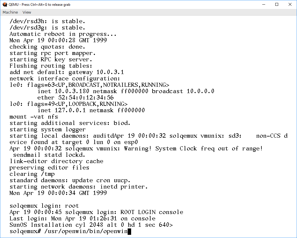
And there, the OS is actually installed! If you are a SunOS/Solaris guru, this is the time to tweak stuff. If not, it's safe to initiate a reboot.
# reboot
For the normal boot, the boot command changes slightly. Now we can tell our "SPARCStation" to just boot off the first disk:
ok boot disk0
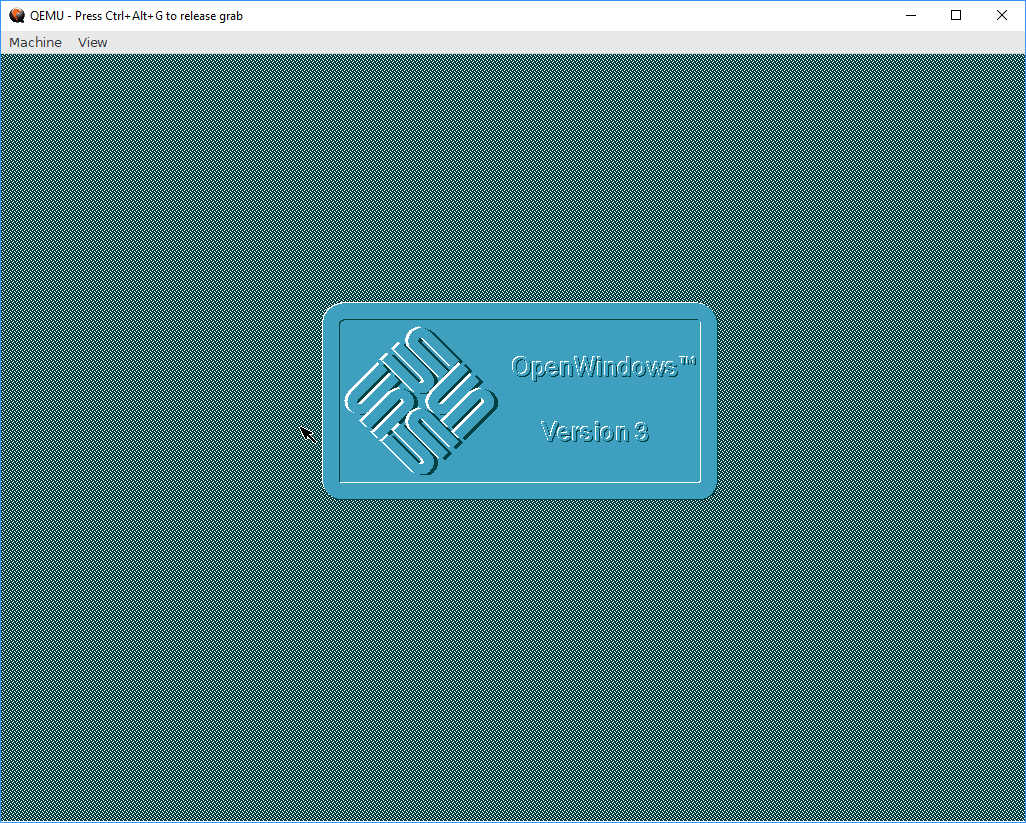
This brings the system up. Logging in as "root" is done without a password, as none is set during install. OpenWindows works, as long as you remember that it's not in path by default:
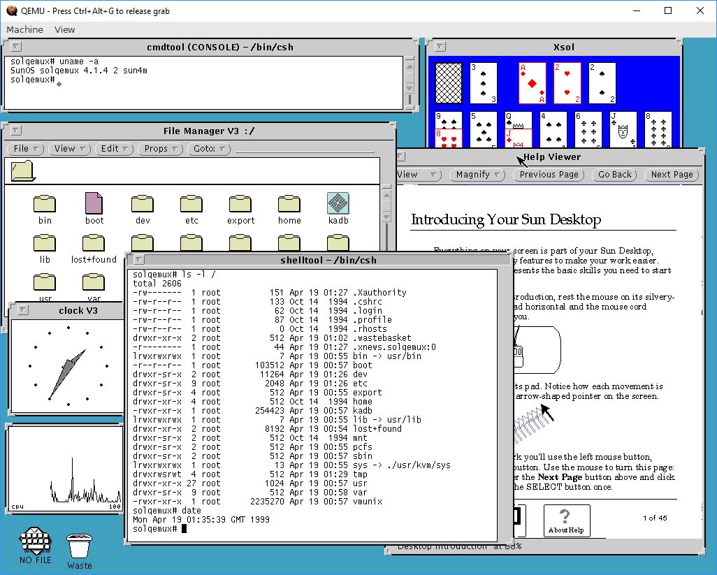
Playing with old and retro stuff is a thing I do. And playing with other architectures than x86/arm even more so. But having to dig out the old, real hardware isn't always possible. For example, it may be winter, cold, and much snow, and the computers may be "frozen in" in the garage. Norwegian winters can be cold 🙂
So being able to do this using QEmu is really a boon! However, I must say that using QEmu on Windows has been one of the least stable and most unpleasant experiences I've had in a while. Keyboard I/O is about 60% reliable, and will lock up in the weirdest ways, constantly. I've had to reset my emulator more times than I can count, just to get to the "suninstall" command, just because I/O has locked up in some way or another. I am going to try this experiment again on Linux, and hopefully my experience will be better there.
Oh, and I tried installing OpenSTEP 4.2 for SPARC. And it REALLY does not want to play ball. It hangs on disk I/O, so I've never actually gotten the installer to start. But it does give some fun warnings though:
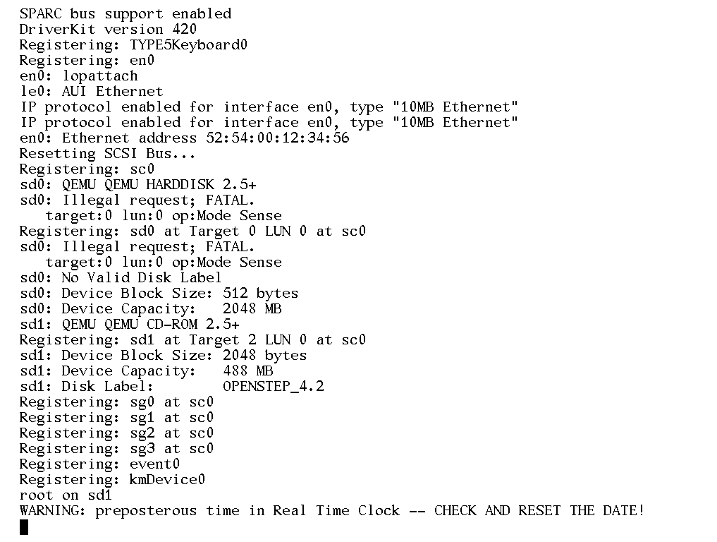
WARNING: preposterous time in Real Time Clock
Adapters and addons to my 8-bit micro
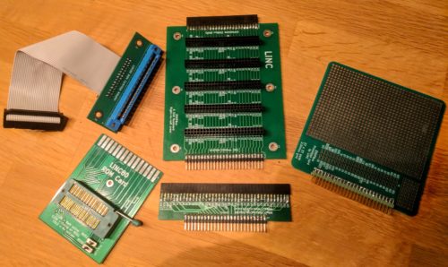
A collection of addon- and adapter cards
While testing my homebrew computer, I made some home-made addons, both in form of perf-board construction and home-etched PCB. I actually also made a connector-on-cable adapter, where I soldered the individual lines of a 30-pin ribbon cable onto an 805-series card-edge connector on one end, and because I failed to properly crimp an IDC connector on the other, I ended up soldering all 30 pins on that side as well. The other home-made adapters I made were: parallel input tester (perf), parallel output tester (perf), adapter from Z50Bus to RC2014 backplane (perf) and ROM Cartridge (PCB).
Considering how good the PCBs I got manufactured for the LiNC80 SBC1 itself, and how much effort went into making the Z50Bus-RC2014 adapter, I decided I wanted to get manufactured a set of support cards for the machine, and make it all look just as good. Additionally, having these support cards available would mean that I could have a small «ecosystem» of parts for future kit availability.
ROM Cartridge
The first card I designed was the ROM Cartridge PCB. The design I sent to manufacture for that was simply a slight tweak of the design I had already etched for testing, so it made sense to complete that first.
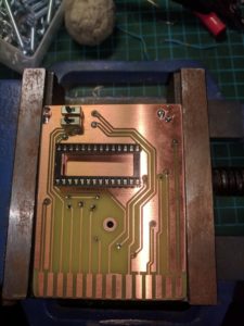 DIY etched ROM Cart |
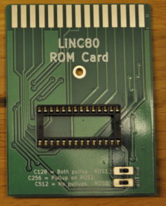 Manufactured ROM Cart PCB |
The card is designed to be large enough to comfortably insert and remove. It has a 28pin location for either a direct soldered or socketed ROM chip, and a central mounting hole for encased cartridges. The two two-position jumper locations allow for any ROM chip size between 16 and 64kByte, taking advantage of the LiNC80 ROM Bank select signals for ROM sizes above 16kByte. If the intended ROM application fits in a 4k or 8k chip, it’s naturally no problem to use chips of those sizes, as the pinout on the connector is JEDEC compliant.
Two jumpers are also on the board, making the choice of ROM chip size flexibility possible, and at the same time giving access to (and control over) the ROM bank select signals on my rom slot connector.
ROM Cartridge Slot
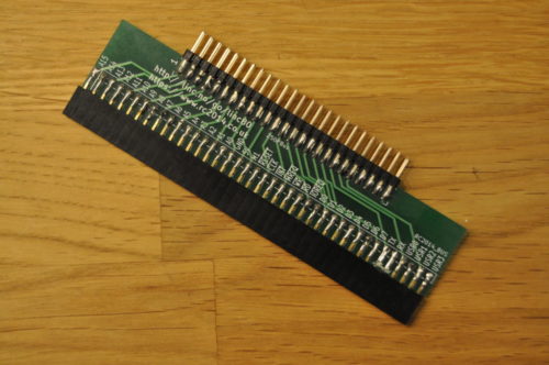
As I mentioned, I hand-soldered ribbon cable onto connectors to test the ROM Slot functionality of my design. Anyone who has tried soldering ribbon cable knows how much pain that is. To anyone who has not tried: avoid it if you can. So to spare anyone else from the unpleasant soldering task, I made up a simple passive IDC-to-Cardedge adapter.
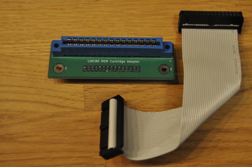
I decided to go with male header pins on the PCB, and use a ribbon cable with female IDC connector on both ends. Mounting IDC connectors can be easily done with a simple vise as a replacement for expensive pressing tools. A simple guide on how to do the vise approach can be found at https://startingelectronics.org/articles/IDC-ribbon-cable/
This is a purely passive adapter, with a pin-for-pin connection for all 30 pins. This means it can also be used as a general pinheader/IDC-to-cardedge adapter in addition to its intended use.
5 Slot Z50Bus
When I first started my design, and came up with the Z50Bus, I realized that I would have to make some kind of bus back-plane card. For this first iteration/version, I decided to make a purely passive one, without any bus buffering built in. I didn't even provide locations for decoupling capacitors, leaving the responsibility for those kinds of things to the expansion cards.
The back-plane has 5 standard slots. Connection to my computer on the right-hand side because the expansion connector on that board is on the left... On the left hand side of the back-plane is an extension header, meaning in theory, multiple cards can be added in a chain.
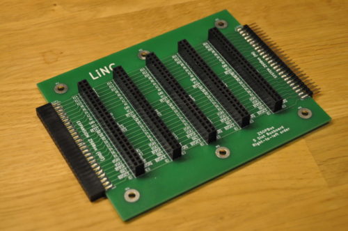
5-slot backplane
Speaking of chains. The Interrupt Chain signals IEI/IEO on this card are connected in a right-to-left order. This makes the first slot be on the right-hand side of the card, closest to the Z50Bus host.
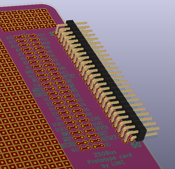
Prototyping card
With a back-plane available, it would be nice to have some compatible expansions. Unfortunately, I hadn't made any of those yet. And I had quite early on realized that my choice of dual-row headers for the bus made prototyping more difficult than if i had gone for single-row. The natural step from this, was to make a made-to-fit prototyping perf-board!
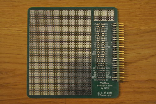
Prototyping card
My board provides a main prototyping area of 27 by 37 individual pads on a standard 2.54mm grid, plus an additional grid of 9 by 5 pads. The 50-pin bus connector is broken out on easily accessible connection points, providing two connecting pads per signal. I chose to make the board exactly 100x100mm. The real reason for this size is that most DIY-friendly board manufacturers have especially low prices for boards up to (including) just that size.
Adapter for RC2014
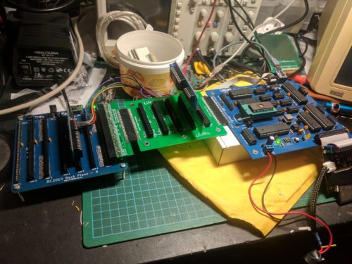
Because I already had built an RC2014 kit, as well as a couple of addons for that system, I felt it made sense to be able to test my expansion bus using those. i had after all designed the bus to be relatively compatible. During building and testing, I created a perf-board version of an adapter, with pin-to-pin wiring. This worked, but it was fragile. In the picture below, you can see this prototype connecting my Revision A computer to an 8-slot RC2014 backplane (not shown is that it works, and runs RC2014 ROM software off the backplane).
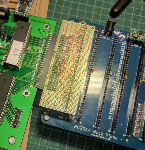
Because this is a trivial adapter, it was a simple design. I tried to compress it without making it DIY-unfriendly. As part of the design, I added pads allowing selection of horizontal or vertical mounting of the RC2014-side of things. On the Z50Bus side of things, I decided to use on-edge mounting of the header simply because I like that style.
Bus-adapter card
I made a mistake in the design of this one. It's not a problem for most add-on cards, but it caused me problems when I tried to test the adapter. My mistake was to wire ALL signals for the simple RC2014 bus straight to the Z50Bus. Including the RX and TX lines. When I tried testing the MC68B50 serial card on the adapter, my system would seemingly not boot. I struggled for a while trying to figure that out, until I realized... The MC68B50 UART and the SIO/2 DUART were both connected to those lines. And both were trying to drive the lines! So my system was booting, but my terminal could not see that, and could not talk to the UART either. By cutting the two traces for RX and TX respectively, I had no problems with any of the modules I had to test. Even running a «Full monty» RC2014 on the RC2014 backplane, using the LiNC80 as just CPU and RAM worked without any issues.
Creative combinations of back-planes, adapters and modules
I may do an update of this board, with jumpers or solder-pads on those two lines, but as long as the user is aware that adding multiple UART chips on the same lines cause problems, I think the current version will work fine.
Before I add my closing line... I am really gearing toward making kits! They aren't quite available for sale yet, but the product presentations and documentation is coming up on my business-site! To start navigation directly from the LiNC80-pages, go to http://linc.no/go/linc80. To see what else I have on offer, see http://linc.no/products, where you also can find the more "official home" of the Z50Bus specification and accessories
This post is part of a series documenting my journey in making my own homebrew computer, the posts can be found on this link.
The birth of my Z80 computer design, the LiNC80 SBC1
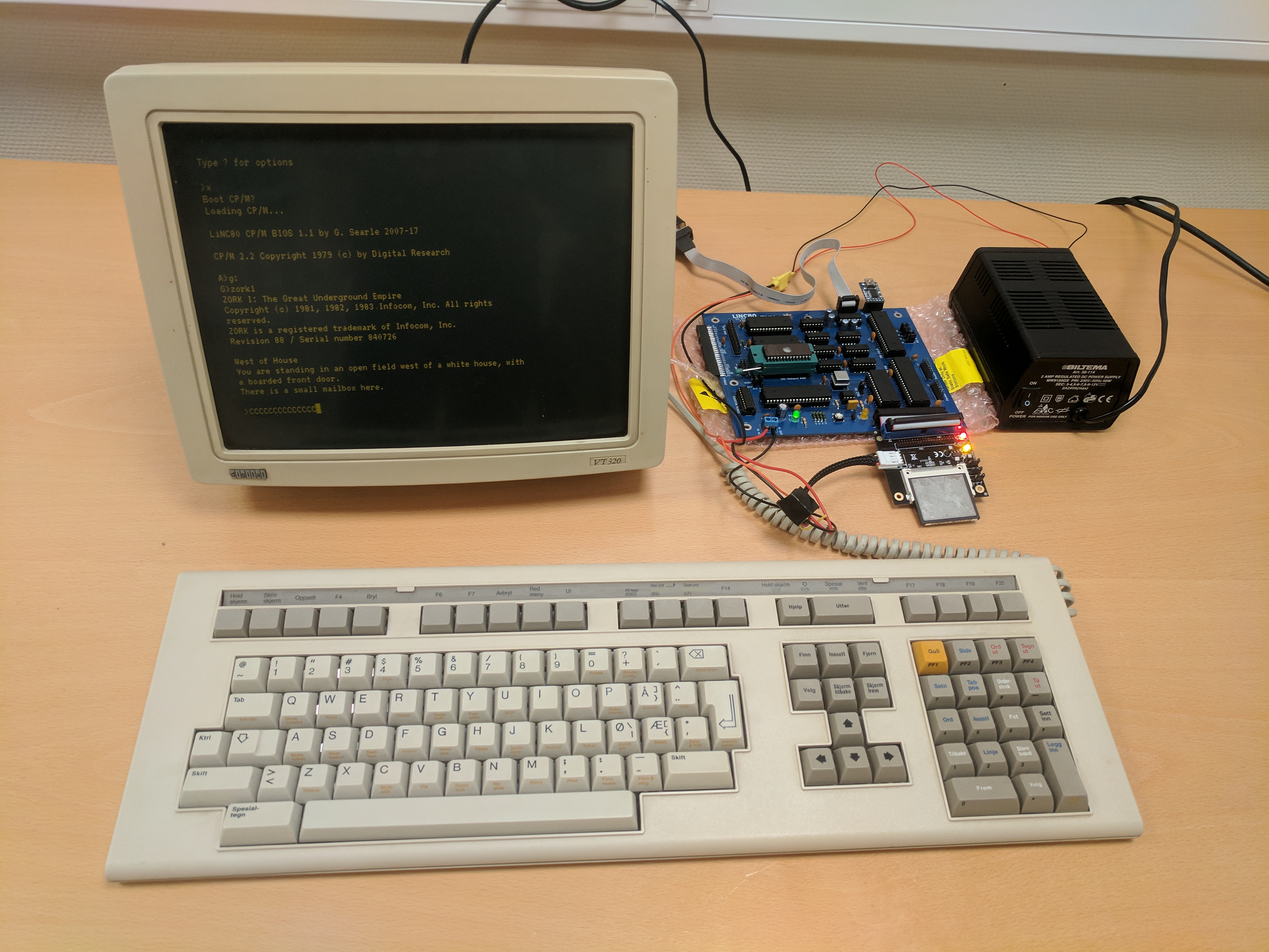
LiNC80 SBC1 Rev C running Zork I under CP/M, using DEC VT320 as serial terminal
I originally started my adventure of homebrew computer building thinking I'd build a relatively simple system. This thought soon changed, as I outlined in the "scribbling ideas" post. The main reason for daring to be more ambitious was basically that with a good base design like the "Fully functional Z80 CP/M machine using only 9 chips" from Grant Searle, and a bit of experience, it seemed to be well within reach! Grabbing the list from the "scribbling ideas" post, my top-level selection of features ended up with this:
- Z80 CPU
- Zilog SIO/2 serial port controller with dual serial ports
- Zilog CTC for four channels of Counter/Timer, 2 of them dedicated to the SIO/2
- Zilog PIO for two Parallel ports
- Expandable system through Z50Bus
- Memory map designed to allow for graphics expansion
- CP/M compatibility
- ROM part of memory from address $0000 disable-able (needed for CP/M and more)
- For fun, a dedicated ROM Cartridge connector
- Z80 Interrupt Mode 2 in the core
- Compatibility with software from Grant Searle (for easy system bring-up)
In addition to that list, I set a limitation of component selection, all active components had to be currently active parts available as new from manufacturer. I also wanted to use static RAM, and have 64KByte of it in DIP packages, so the design uses two 32kx8 SRAM ICs.
I'm really not much of a software-guy. I can program, and I know my way around assembler code, but I am most definitely not one of those guys that can code a ROM Monitor in an evening. Being able to re-use existing software helps me get my system up and running. The fact that Grants software works well, on a system that can run an operating system I want to use, means it would be silly of me to not take advantage of that. Because that existing software uses IM2, I would have to use IM2 as well, or commit to some serious software redesign. Besides, I wanted to try out IM2 more because I think it's cool. My desire to run CP/M also dictates the need to have a way to disable (or move) ROM out from address $0000 of the memory-map.
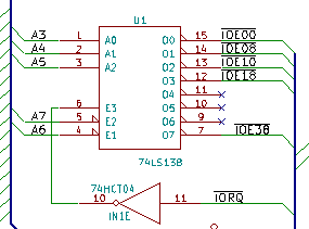
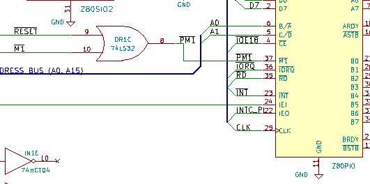
The "dependency effect" of using existing code also makes itself visible in hardware I/O address selection. To avoid changing too much code, it makes sense for me to place the SIO/2, ROM-disable and CF-disk I/O addresses on the same addresses used in Grant's design. I also liked his approach of using a 74LS138 for decoding, so I stuck with that approach, and selected "remaining" decode outputs for use with the CTC and PIO. The decoding logic ends up "eating up" 8 I/O addresses for each "on-board device", so 40 I/O addresses in the ranges 0x00 to 0x1F and 0x38 to 0x3F are locked. Somewhat expensive in terms of resources, but it allows for a simple construction with few parts. Besides, all addresses from 0x40 and up to 0xFF are still available for expansions.
I/O address decoding for on-board devices
As listed, I wanted to be able to use software-controllable bit/baud rates on the serial ports. To be able to do that I chose to include the Z80CTC, a counter/timer controller, to drive the SIO. But I wasn't quite sure about my Z80 assembly skills yet, so I decided to include a jumper-selector to select SIO-clock to be CPU clock or CTC. That way, I could select CPU-clock for booting unmodified code from Grant, and then switch to CTC-clock once I knew how to do that.
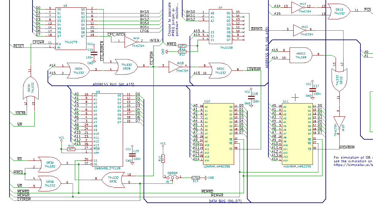
My first major divergence from the base design came as a result of my desire to have a memory map designed for graphics. Being able to combine that with the option of running code other people has made for Grant's design, meant that I had to include some kind of bank-switching. The design already included a very basic form of bank-switching: Grant has designed the "disable ROM" feature as a simple RS-latch that bank-switches the lower 16k between ROM and RAM. To switch from the ROM bank to the RAM bank, a write to address 0x38 needs to be done. In his design, the bank switch is triggered by an I/O write to the correct address, and the data is not used for anything. I examined the source code and found out that even if you only need to write something to the address, his code actually writes the value 0x01. Based on that, I decided that my "memory management" for bank-switching could be done using some kind of register, placed at 0x38, as long as the lowest bit of the register was used for enabling/disabling ROM. This would additionally give me the option of switching ROM back in, in contrast to Grants design where only a system reset would bring ROM back into active memory.
Armed with a general idea on how I could do bank-switching, I started looking at how I could make a memory map that worked with both CP/M and graphics. Because CP/M needs to have its BIOS and BDOS placed in a predictable, always available location in memory, and it expects RAM in the bottom of memory, my options were a bit limited. On top of that, I wanted to at least start with existing software, and the software I had available expected to be able to stuff BDOS, BIOS, ISRs and stack in the top 8-16k of memory. That made me decide to use a fairly odd and uncommon memory map. I decided that the second-top-most 16k would be the "window" for bank-switching. Basically, bottom 16k is switchable RAM/ROM, second 16k is always on-board RAM, third 16k is switchable memory defaulting to on-board RAM, and fourth and final 16k is always on-board RAM.

Memory map / layout for LiNC80
With the general memory map laid out, I turned my attention back to that register I talked about earlier. I decided I'd go for the simplest approach I could think of, one that I had used to implement a simple digital-out solution for the RC2014 computer. By using a 74LS273, I could get a very simple 8-bit write-only register. To quote the data sheet: «The SN54/74LS273 is a high-speed 8-Bit Register. The register consists of eight D-Type Flip-Flops with a Common Clock and an asynchronous active LOW Master Reset.». Placing one of those on I/O address 0x38, using IO Write as clock input and the data bus as D-inputs, I could use the outputs to perform bank switch selection. Using the system RESET signal for the '273s Master Reset, the system would always reset to a predictable state. And by using the lowest bit to control ROM disabling, I had compatibility with the existing code from Grant! With seven bits still available, I decided to use three bits for RAM bank select. This would let me simply use another LS138 to select one of eight RAM banks, and by using "location 000" for the on-board RAM, things should boot nicely.
I selected to use one bit of the "register" to control Interrupt Enable Input of onboard devices. This would let me "lock" interrupts to an IM2 disabled state, a feature I thought would be handy to have on top of the Interrupt Enable / Disable Interrupt instructions of the CPU. This left me with a few bits left over. In my scribbling, the idea of having a ROM cartridge for fun and experimentation had been added. I quickly added to that idea, by using two of the bits as "off-board ROM bank selects". That would allow a ROM cartridge to have four 16k banks! Which by the way matches nicely with a standard 64Kbyte ROM chip size.
With memory map idea fleshed out, I had to figure out a way to make the memory decode and interfacing work. I ended up finding a cool tool at https://simulator.io/ that allows for on-line simulation of digital logic. Using first a set of logic tables, I assembled an idea, and implemented it on simulator.io first, before adding it to my design. You can see and play with the result at https://simulator.io/board/RoLQ8QDEei/2. Confident that I had a memory layout that could work, and a decode logic that seemed to make sense, I started the actual design. The resulting memory interfacing logic took quite a bit more glue logic than Grants simple design, but I think it came out quite nice.
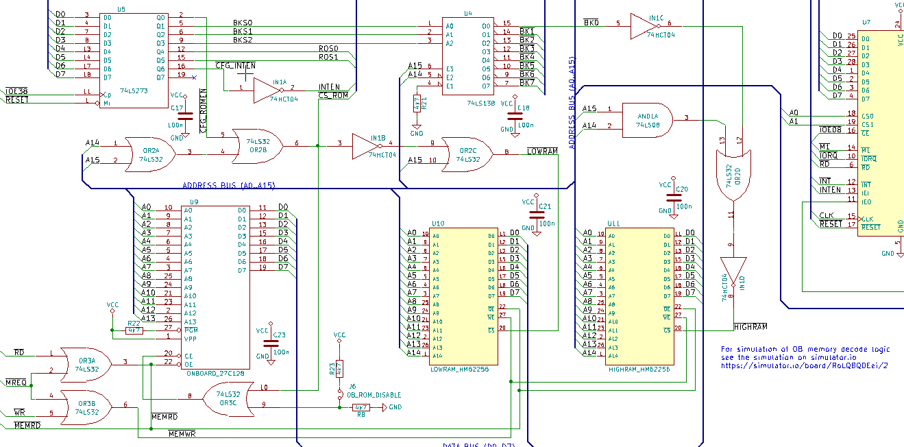
Memory logic Revision A of my Z80 design (with flaws)
The overall schematic I had in KiCAD was at this point starting to get large and complex. Thinking back at my issues with flaky breadboards, I was starting to dread building something as complex as this on either wonky breadboards, or on a very large perf-board. It would be doable, but the thought of debugging soldered point-to-point or bad breadboard connectors didn't really sound tempting. At the same time, I was still learning to use KiCAD for a somewhat large design, and I more or less accidentally started laying out a PCB. Combining manual parts layout, a bit of manual routing and experimentation with freerouting, I suddenly had a board layout that looked decent. So I took a gamble, and simply sent off some money and a few gerber files to seeed studio. Not a full week later, I received a box containing five fine looking PCBs.

This board was designed with all the bullet points from the design list. There's SIO/2, CTC and PIO devices, an IDE connector, and on the right side, a Z50Bus expansion bus. Additionally, I created a different version of an expansion connector on the left side that included all the decoded bank-switching lines (but not all CPU-signals, to keep it on a 50-pin connector).
Seeing how nice my PCB looked, I got to work assembling it. I soldered in passives, added sockets for IC's, and completed all soldering. After some experience with how much rosin flux can affect a complex logic circuit, I cleaned the board thoroughly before adding any of the semiconductor components. Finally, I hooked up serial ports and applied power.
Nothing happened.
Or, well, something happened. The board started drawing current, and it was well within expected range. So it would seem that the reason for it not working wasn't a dead short or a major defect. It had to be some kind of logic design flaw. I got a hold of a cheap logic analyzer to try to figure out what was wrong, but I couldn't get the analyzer to trig properly on the T1-T3 multi-clock-per-instruction that the Z80 has. I shelved the project in frustration for a while. After some months of not working on it, I brought it back out, and started poking around. After seeing some weird behavior, and a bit of "almost working" if I removed both the 'LS138 and the 'LS273, I figured something was weird with the I/O addressing. On examining the schematic in detail, I realized I had made two really silly mistakes.
The I/O address decoder was always active, doing its decoding even on Memory operations and even on the built-in DRAM refresh. Next, the 'LS273 that I was using as my "configuration register" only used the I/O address decode signal as its "Write" signal! These two problems together meant that the contents of the "register" was constantly changing. I'm not surprised that the code in ROM was less than happy about getting bank-switched out half-way through an instruction... Fortunately, I had spare logic elements in the glue logic IC's. This allowed me to fix the problems using bodge-wires and cut traces on the back of the PCB. The same evening I discovered my errors the system started doing what I had intended, and I had working CP/M on my slick-looking homebrew PCB.

I decided it would be best to fix the mistakes in my schematic, so I went back to KiCAD and implemented the changes that I had made on the board. I swapped some gate selection around to make the glue logic easier to route. While I was looking at the routing issues, I had a long think about the whole "two expansion ports, one for system and one for graphics". In the end, I decided it did not really make sense. I could put all the memory/bankswitch and graphics-only signals on a much smaller header connector, and use a cable to a standard Z50Bus expansion card. That would mean only one expansion connector would be needed. This in turn would lead to much simpler routing of the board, and the board could be physically smaller, reducing cost.
Reducing cost may sound weird. After all, this is my homebrew design, and I already had a working computer in front of me. But at this point, I was seriously considering making this a kit. And if I was to sell any of these, making the cost of the PCB go down would be a good plan. So, the changes were implemented, I did a new layout, and sent it off to seeed for fabrication. 10 days later I got a new batch of boards that I fairly quickly assembled. I transplanted all ICs from the previous build over, and tested it.
And it did not work. ARGH!
Back to the schematic, I found ONE silly mistake. While I was redesigning, I had done some changes to the schematic around the SIO/2 chip, and while doing that, I had swapped the address lines A0 and A1 by accident. That meant that the Control and Data addresses had become swapped. A quick cut-and-solder on the PCB swapped those back, and the computer came to life! I set to work writing code to test the other on-board devices that aren't on Grants design. I got the CTC to clock and generate interrupts, and I got the PIO to work as Byte-out, Byte-in, and bit-in-out. But no matter what I did, I could not get the PIO to generate interrupts.
It turns out, the PIO interrupt signal is gated by its M1 input. And, because the PIO actually has one pin less than it needs, Zilog chose to make a multiplexed M1+Reset function on the M1 pin. And in my design, I had thought "M1 input is active if either CPU M1 is active OR if system Reset is active". So I had put an OR gate there. There's one problem with this. Both Reset and M1 are ACTIVE LOW signals. And to make an "or" function for active low signals, you need to use an "and" gate! Long live boolean logic and active low signals. Who would have thought OR to be different from AND in boolean logic... I managed to finagle this by more bodging, and eventually I had a fully working computer, where all on-board devices worked.
Considering the amount of self-inflicted troubles I had experienced so far, I decided to test the expansion bus and the ROM cartridge connections before fixing my schematic again. To my relief, both of those worked without problems. I was able to use a ROM cartridge with ROM bank select, and was even able to use the RC2014 backplane to test using off-board memory and off-board devices.
During the testing of the ROM cartridge solution, I discovered that the rule of only using parts still in production had been violated on my design. I had based the on-board ROM circuit on a 16Kx8 EPROM, the 27c128. That ROM chip is not available, and neither is it's EEPROM-version, the 28c128. Fortunately for me, the bigger AT28C256 is still in production, and very close to pin compatible. I revised the schematic and board to include two jumpers for on-board ROM allowing either tied VCC signal for 'c128-devices, or use of the ROM-select lines. This makes it possible to select between 'c128, 'c256 and 'c512 ROM chips (16k, 32k and 64k), and even use of bank switching for on-board ROM. The physical placement of the jumpers was done so a ZIF-socket would fit (it's tight, but it fits), just because I could.

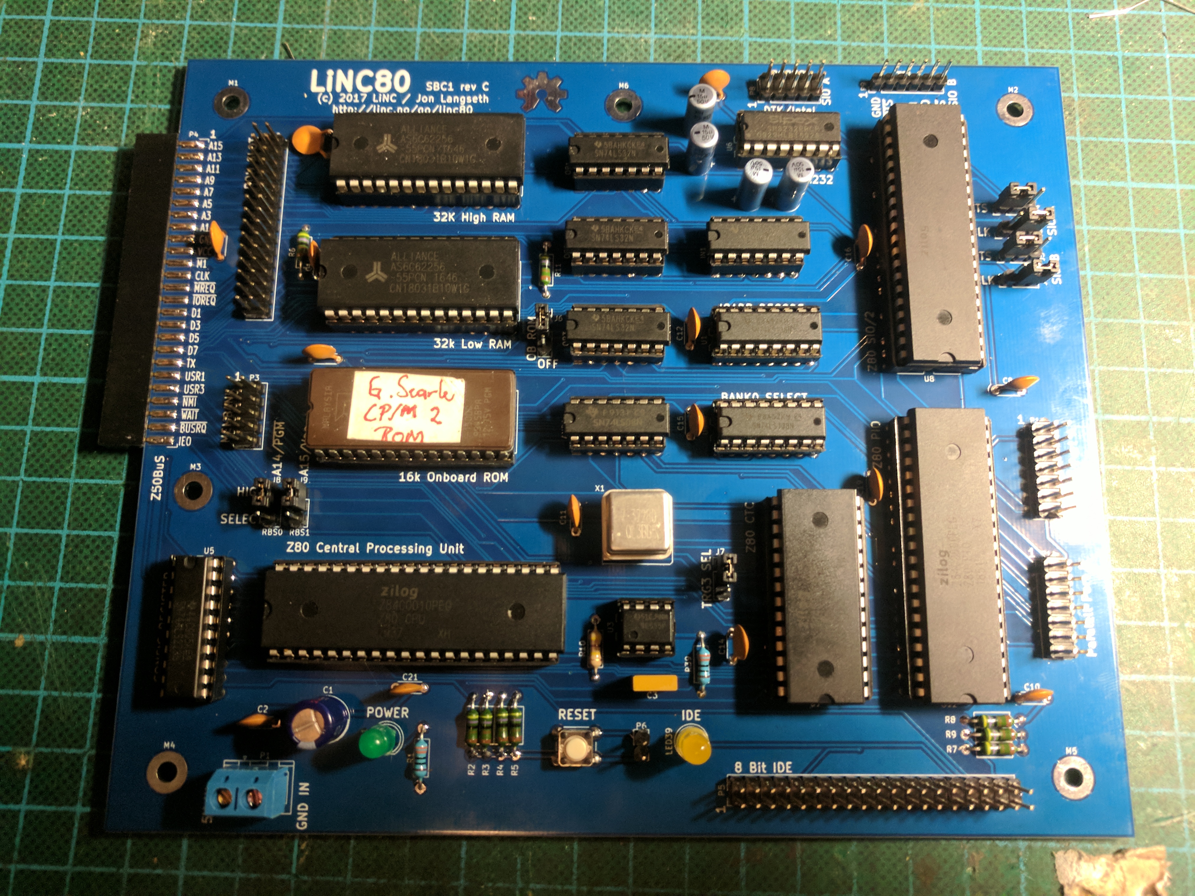
Considering the errors in this revision B of the board, I made corrections, and created revision C. This board now carries my official name for my homebrew computer design as it stands today: the LiNC80 Single Board Computer 1 Rev C. Considering it is an expandable board, with no on-board graphics, it may seem strange that I call it an SBC. Before the arrival of a heap of BeagleBoard and Raspberry Pi like devices, it was usual to call a PCB that implemented a fully working embeddable computer an SBC, and it was unusual for SBCs to have local graphics, but not unusual for them to have expansion/interface connectors.
Revision C of the board still has a minor issue, but none that makes a real difference to a system user that is aware of it. The only significant problem I see at the moment, is related to how the two serial ports behave on RTS/CTS signals if one of the ports is left unconnected. On the board, there is a jumper that selects between honoring incoming CTS (RTS from other host), or tying it to Gnd. If unconnected and not tied to Gnd, the SIOA tends to lock up the second serial port SIOB. On the other hand, if SIOA is connected, but SIOB is left unconnected, random characters may get generated if the CTS input is floating. The solution is to jumper the unused CTS signal to "disabled" for an unconnected SIO port.
This post is part of a series documenting my journey in making my own homebrew computer, the posts can be found on this link. Stay tuned for more posts in this series. The next will probably be about the various adapter cards I have planned/made.
Note! I am gearing toward making kits available!
The product description pages for the kit starts off at http://linc.no/products/linc80-sbc1/
The new, more official page for the Z50Bus is located at http://linc.no/products/z50bus
Xen on Debian Stretch (with VLAN networking).
This is an update to my old post about Xen on Debian Wheezy. The process of getting my configuration of Xen running on Debian 9 is very close to the old approach, so I'll only cover the differences.
I've recently been "forced" to update my Xen setup. The setup has been working great for me, and is still working great. But recently I really need to get some Stretch, CentOS and Windows VMs up. The old versions of Xen and pygrub in Wheezy refuses to boot the modern kernels for Linux, and the machine I use as host is unable to du HVM for Windows. And Wheezy is getting really old, and is soon getting dropped out of support.
Installing Xen
The primary install command is still exactly the same as it was before:
apt-get install xen-linux-system
In the old guide, I next described how one would get Grub to automatically boot into the Xen kernel. This is not needed on Stretch, the Xen hypervisor kernel is automatically set as the defaul boot option when it gets installed.
The points about memory allocation and balooning still apply, but the memory requirement is a little bit higher. I recommended reserving 768MB to dom0 on Wheezy. This will work and let you boot and stuff with Stretch, but it will be a bit tight. So upping the reserved allocated memory to a full GB makes sense.
Adding the kernel-option to 'fix' the memory size:
cat <<END >>/etc/default/grub
# Xen boot parameters for all Xen boots
GRUB_CMDLINE_XEN="dom0_mem=1024M"
END
update-grub
Edit /etc/xen/xend-config.sxp and change the dom0-min-mem and dom0-ballooning lines:
(dom0-min-mem 1024)
(enable-dom0-ballooning no)
Network configuration
There are a few changes to the network setup. One of the more visible changes in configuration files is that Debian is no longer using "legacy names" for network interfaces, instead presenting systemd predictable names. And with this switch to systemd, the familiar command "ifconfig" has been dropped completely, forcing us to move to the much more useful "ip" command.
Next, having dummyX network interfaces now require that you set them up before you try to use them in /etc/network/interfaces. You can use a dummy-interface manually after boot by simply creating it, but to have it available on boot, you need to load the module explicitly. Add the following to /etc/modules:
# /etc/modules: kernel modules to load at boot time.
dummy
Next, we need to specify how many dummy-devices we want as a module load option. Create the file /etc/modprobe.d/dummy.conf with a single line:
options dummy numdummies=1
Of course, if you want multiple vm-to-vm local network bridges available, increase the numdummies as desired.
My /etc/network/interfaces is fairly verbosely commented, so again, I'm including it directly, and letting it speak for it self. Remember to install bridge-utils to get working network bridges.
# This file describes the network interfaces available on your system
# and how to activate them. For more information, see interfaces(5).

# The loopback network interface
auto lo
iface lo inet loopback

# The primary network interface, used for management and in the future, iSCSI
# In my setup I'm actually using DHCP for address, with the address locked down
# on the DHCP-server side..
allow-hotplug enp3s0
iface enp3s0 inet dhcp
iface enp3s0 inet6 auto

# Create a dummy interface to use with a "local-only"
# bridge to use for domU-to-domU pure local traffic
auto dummy0
iface dummy0 inet manual
	pre-up ip link set dev $IFACE up
	post-down ip link set dev $IFACE down

# Bring up the NIC for VM networks, but with no address configuration
# The interface will be used later as a bridge-port interface.
# It is also connected to a switchport that does VLAN
# trunking with native (untagged) VLAN 2 and VLANs 3,4 and 5 tagged.
auto ens2f0
iface ens2f0 inet manual
	pre-up ip link set dev $IFACE up
	post-down ip link set dev $IFACE down

# VLAN CREATION
# Creating VLANs has become a lot better in Wheezy.
# All that is needed to create a VLAN subinterface now,
# is to add a stanza for a eintfX.Y subinterface. Y becomes
# the VLAN ID.

# Adding VLANs tagged on eth1. These are simply
# brought up, they will be added as bridge-ports later.

auto ens2f0.2
iface ens2f0.2 inet manual
	pre-up ip link set dev $IFACE up
	post-down ip link set dev $IFACE down

auto ens2f0.3
iface ens2f0.3 inet manual
	pre-up ip link set dev $IFACE up
	post-down ip link set dev $IFACE down

auto ens2f0.4
iface ens2f0.4 inet manual
	pre-up ip link set dev $IFACE up
	post-down ip link set dev $IFACE down

auto ens2f0.5
iface ens2f0.5 inet manual
	pre-up ip link set dev $IFACE up
	post-down ip link set dev $IFACE down

# BRIDGES
# Add the bridge for pure local-only communication between
# domU's. Just for fun, I'm setting an IP on this interface..
auto xenlocal
iface xenlocal inet static
        bridge_ports dummy0
       	address 192.168.127.2
	netmask 255.255.255.0
	bridge_stp off

# None of the interfaces below have IP addresses assigned. Any domU hosts using
# these are not supposed to use the bridge for direct communication with dom0.

# The configuration for the VLANs is very repetitive: An 'auto' line to make
# sure the interface comes up automagically, an 'iface' line setting the bridge
# name and defining it to 'manual' configuration, definition of the VLAN
# subinterface, and finally setting Spanning Tree to 'on'.
# If even more control over the bridge interfaces is needed,
# read 'man 5 bridge-utils-interfaces'

# For the VLANs, I used 'vlanX' as bridge-name
# ens2f0 is used as physical-interface for both untagged and for tagged VLANs,
# please review the separate ens2f0 and ens2f0.X definitions above, and separate
# vlanX bridges below.

auto vlan2
iface vlan2 inet manual
        bridge_ports ens2f0.2
        bridge_stp on
	bridge_maxwait 0

auto vlan3
iface vlan3 inet manual
	bridge_ports ens2f0.3
	bridge_stp on
	bridge_maxwait 0

auto vlan4
iface vlan4 inet manual
	bridge_ports ens2f0.4
	bridge_stp on
	bridge_maxwait 0

auto vlan5
iface vlan5 inet manual
	bridge_ports ens2f0.5
	bridge_stp on
	bridge_maxwait 0
Getting Debian Xen Netinstall data
I've updated my "update-debian" script to make adding and removing releases easier. The new version does the same as the old one: It pulls down the Xen kernel and initramfs images for Debian netinstall from the Debian servers.
#!/bin/bash
DEBINSTROOT=http://cdn.debian.net/debian/dists/
DISTROS="wheezy jessie stretch"
for DIST in ${DISTROS}
do
 for ARCH in i386 amd64
 do
 mkdir -p /srv/xen/boot/debian/${DIST}/${ARCH}
 for FILE in vmlinuz initrd.gz
 do
 wget ${DEBINSTROOT}/${DIST}/main/installer-${ARCH}/current/images/netboot/xen/${FILE} \
 -nc -O /srv/xen/boot/debian/${DIST}/${ARCH}/${FILE}
 done
 done
done
Creating virtual machines (domU)
In the old post I described how to use some pre-built templates for creating virtual machines. I have generally not used that approach, so I'm not updating that doc. The "official" way of creating new virtual machines seems to be using xen-tools for deployment, or some libvirt magic. Sounds great, I haven't tested it 😀
My way of creating machines is simply to copy a template configuration, and run the installer. My updated template is more or less identical to the old one:
name = "hostname"
memory = 512

# Let xm/xl allocate MAC-address on first boot:
vif = ['bridge=vlan2']
# Get MAC-address from first boot, and update:
#vif = ['mac=xx:xx:xx:xx:xx:xx,bridge=vlan2']

disk = ['file:/srv/xen/hostname_root.img,xvda,w']

# During install, use the erknel/ramdisk/bootloader lines
kernel = "/srv/xen/boot/debian/stretch/amd64/vmlinuz"
ramdisk = "/srv/xen/boot/debian/stretch/amd64/initrd.gz"
extra = "debian-installer/exit/always_halt=true -- console=hvc0"

# When install is done, remove those, and switch to pygrub or pvgrub
bootloader="pygrub"

# Select what to do on a reboot:
# stop the VM as if a HALT was done, or actually restart.
on_reboot = 'destroy'
#on_reboot = 'restart'

# You can select to auto-restart a VM that crashes.
# I prefer to manyally handle crashes.
on_crash = 'destroy'
The absolute minimum amount of RAM needed to boot the Debian 9 installer is 450MB. I discovered this the hard way, simply because my old template used 384MB RAM as the initial allocation.
This template uses qemu-diskimages, not LVM volumes or such magic. Creating the disk image is as before:
qemu-img create -f raw /srv/xen/hostname_root.img 10G
The toolstack has been changed from xm to xl
Along the upgrade-path from Xen 4.0 to the current 4.9 version, the older "xm" toolstack got replaced by "xl". This really does not make much difference in simple use, as the commands are more-or-less interchangable. My cheat-sheet for commands generally only substitute "xl" where it used to be "xm". Discovering what NIC and MAC-address has been allocated to a VM is now done easily with xl, so poking around in xenstore-ls is no longer needed:
# I use the machine's FQDN as it's domU domainname.
# So, in examples, replace hostname w/Xen domU domainname

# Start VM, don't attach to console
xl create /etc/xen/guests/hostname.cfg

# Start VM, attach to console immediately
xl create -c /etc/xen/guests/hostname.cfg

# Attach console to a running domU/VM
xl console hostname

# To get out of the console again, CTRL+5 is still used.

# Kill a running VM, unclean brutal shutdown
xl destroy hostname

# List running virtual machines/domU's
xl list

# List network adapters (inc MAC) of a given domU
xl network-list hostname

# Real-time status, TOP for Xen
xl top
References and pointers.
This is an update to my old post about Xen on Debian Wheezy. There is more than a little information there that I haven't covered here, because the old info is still correct.
A bit of info on the new-style network interface names can be read at https://major.io/2015/08/21/understanding-systemds-predictable-network-device-names/
General documentation links
For more references, simply refer to the old post 🙂
Z50Bus – A compact expansion bus for 8-bit microcomputers
Note!
The new, more official page for the Z50Bus is located at http://linc.no/products/z50bus
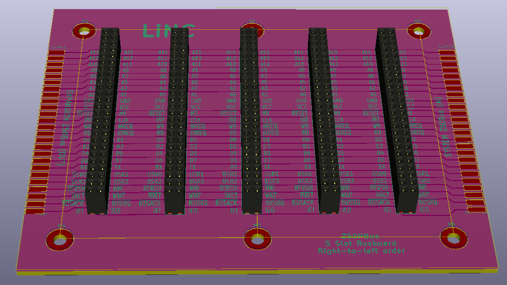
A 5 "slot" Z50Bus backplane
The Z50Bus is a suggestion for a system expansion bus for 8-bit microcomputers. First, a little background. It came into existence early in my design phase of my own homebrew computer. As such it is a new bus layout, and my personal needs is reflected in its layout. I wanted an expandable system, I wanted it to have a documented bus layout to allow others to design around it, the bus should be electrically simple, and require few logical components to implement. To satisfy the criteria of being simple and require few components, the layout needed to be close to the CPU I intended to use. As a result of that, the bus is closely tied to the CPU signals of the Zilog Z80 CPU. I investigated using an existing bus layout. The standardized bus layouts that I found to be relevant were S100[1][2] and STD80[1][2] or the 56-pin variant of the STD bus, as used by the Ferguson Big Board II shown at the bottom of this post. In my opinion, using any of these would require more complexity than I wanted. Following the actual standards would also be required, which would require the use of 100-, 80- or 56-pin edge connectors, and including voltage levels that seem weird in modern systems. Most of +8V, +16V and -16V, +12V and -12V would need to be included. I also looked to the popular homebrew kit system RC2014. Its bus layout is very simple, and with a SIL-like connector, it's very easy to make prototypes for the system. What I don't like about the bus, is that the standard version does not implement all useful CPU signals, and the physical rigidity of the connectors is weak. So, I wanted to use a pin-header based connection that is more rigid than a single row, and at the same time let the width of the physical connection be fairly small.
The name of the Z50Bus comes from being originally designed to use a 50-pin connector to integrate a system around a Z80 CPU. Being a simple bus specification, it is possible to use/integrate it with other 8-bit CPUs using some glue logic. One such example is shown later, for using a 65C02 CPU.
Signal levels and descriptions
Signal levels are 5V Single Ended, with HC TTL levels expected. So, each signal uses a single line, and an active high signal will have a High at 3.5V - 5V, and a Low state at 0-1V. The 5V and GND lines are the only supply voltages on the bus. System implementations should make sure these are noise-free, well decoupled, and dimensioned for the system current draw.
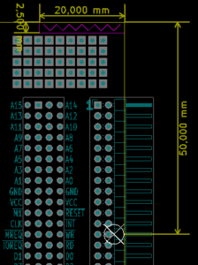
The bus uses a double-row connector scheme, with the following pin layout
| Pin | Signal name | Pin | |
| 1 | A15 | A14 | 2 |
| 3 | A13 | A12 | 4 |
| 5 | A11 | A10 | 6 |
| 7 | A9 | A8 | 8 |
| 9 | A7 | A6 | 10 |
| 11 | A5 | A4 | 12 |
| 13 | A3 | A2 | 14 |
| 15 | A1 | A0 | 16 |
| 17 | Gnd | Gnd | 18 |
| 19 | 5V | 5V | 20 |
| 21 | /M1 | /Rst | 22 |
| 23 | Clock | /Int | 24 |
| 25 | /Mreq | /WR | 26 |
| 27 | /IOreq | /RD | 28 |
| 29 | D1 | D0 | 30 |
| 31 | D3 | D2 | 32 |
| 33 | D5 | D4 | 34 |
| 35 | D7 | D6 | 36 |
| 37 | Tx | Rx | 38 |
| 39 | Usr1 | Usr0 | 40 |
| 41 | Usr3 | Usr2 | 42 |
| 43 | /NMI | /Refresh | 44 |
| 45 | /Wait | /Halt | 46 |
| 47 | /BusRQ | /BusACK | 48 |
| 49 | IEO (*) | IEI (*) | 50 |
Female bus - Male card
* Note that IEO/IEI forms an Interrupt Enable Chain, where the IEO of a higher priority card needs to connect to a lower priority card. This means a bus board needs to connect IEO of one "slot" to the IEI of the next. It also means cards need to be present "in order", or empty slots need IEI/IEO jumpered for interrupts to work.
This layout of the signals is relatively simple to lay out for both CPU and expansion cards. Additionally, it is easily "unfolded" onto a single-row implementation, where using the first 42 pins mapped onto a 1x40 connector gives full compatibility with the bus layout of the RC2014 compatible ecosystem.
The on-bus signals function/description closely follow Z80 CPU signals, with a few extra signals inspired/compatible with the RC2014 signal set:
| D7..D0 | Data bus lines |
| Clock | System / CPU Clock (Phi2Out for 6502) |
| /Rst | System Reset, Active Low |
| /Mreq | Memory Request, Active Low, CPU Output |
| /IOreq | IO Request, Active Low, CPU Output (synthetic for 6502) |
| /WR | Write, Active Low, CPU Output |
| /RD | Read, Active Low, CPU Output |
| /M1 |
Machine Cycle One, Active Low, CPU Output (M1+IORQ active indicates INTAck. May use SYNC on 6502)
|
| /Int |
Interrupt, Active Low, CPU Input, device requests interrupt by pulling INT low.
|
| /NMI |
Non Maskable Interrupt, Active Low, CPU Input, device requests interrupt by pulling INT low.
|
| /Wait |
Wait, Active Low, CPU Input, used to hold the CPU for wait states (can integrate RDY for 6502)
|
| /Halt |
Halted, Active Low, CPU Output, indicates that the CPU is in WAIT FOR INTERRUPT state (HALT or WAI instructions)
|
| /BusRQ |
Bus Request, Active Low, CPU Input, used to request bus control, i.e. for DMA
|
| /BusACK |
Bus Acknowledge, Active Low, CPU Output, indicates that a BusRQ is accepted, and that CPU signals are high-Z
|
| /Refresh |
DRAM Refresh cycle, Active Low, CPU Output. When Refresh and Mreq are active, a DRAM refresh can be done
|
| IEO (*) |
Interrupt Enable Out, Active High output from one expansion card to next expansion.
|
| IEI (*) |
Interrupt Enable In, Active High input to expansion from previous expansion card or system/CPU board
|
| Tx / Rx | System internal TTL Serial |
| Usr0..Usr3 |
User Definable pins (USER1...4 on RC2014, note numbering difference)
|
The signal layout for Z50Bus is simplistic, and makes very little attempt at being a signal balanced and noise cancelling bus design. The bus specification itself does not indicate if a system should use buffered bus or buffered expansions (or be raw CPU signals).
Mechanical implementation and suggestions
The standard bus connector to be used, is 50-pin dual-row header pin and socket, with 2.54mm pin pitch. For expansion cards that plug into a busboard, a Male pin header with nominal 6mm pin length should be used ("standard" header, sometimes called 11mm). The bus-side connector should be a Female PCB Header Socket, with nominal 8.5mm height.
The suggested arrangement for expansion cards is to use a Right angled connector. For orientation, an expansion card laid out so the connector is on the right hand side should have pins 1 and 2 as the top pair, 49 & 50 the bottom, and the connector on the component side.
Mechanical layout is not strictly bound by the bus layout and design, but to allow for card supports, the following suggestions apply. On an expansion card, the center pair of pins (and thus the center of the connector) should be located 50mm from the edge closest to the connector pins 1 & 2. The card should leave space for a support raiser going 2.5mm in from the edge closest to pins 1 & 2, extending 20mm along that edge.
 Connector on expansion card for Z50Bus |
 Position of connector |
For connectors used to connect a system board and expansion or bus-board, the suggested arrangement is to use straight connectors placed on-edge, female connector on the system board (main bus) side, and male on the expansion (exp bus) side. This allows the main-bus card and the exp-bus card to lie in the same plane, without requiring expensive right-angle 2x25 socket headers.
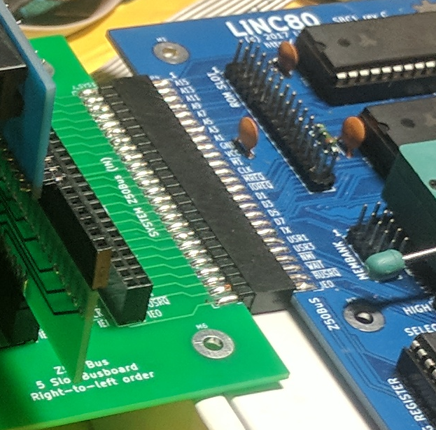
Example of on-edge connectors for joining a system board (right, female connector) to an expansion bus board (left, male connector)
Using the Z50Bus with the 6502
Being a bus for 8-bit microcomputers designed after 2016, the number of potential CPU's relevant for new designs is limited. Currently only the Z80-family and the 65x02 family of CPU's have parts still in production. Because of this, only a 65x02 adaption of the bus is suggested here.
Some of the Z80-style signals need to be synthesized. 65x02 uses memory mapped IO, so the IOReq signal needs to be generated by the CPU card/system when a request is made to the 65x02 IO address space selected for the system. The Mreq signal will then be a simple invert of the IOReq signal. An equivalent function of the WAIT and HALT signals may be found on the 65x02 RDY line. A diode split of the function may be appropriate. The SYNC signal can be adapted for the M1 signal function, if the INTAck feature is considered in the implementation.
| 65C02S signal | Z50Bus | Z80 signal | RC2014 |
| *SYNC | M1 | M1 | N/A |
| (generated) | MREQ | MREQ | MREQ |
| (generated) | IOREQ | IOREQ | IOREQ |
| *R/W | RD | RD | RD |
| R/W | WR | WR | WR |
| N/A | RFSH | RFSH | N/A |
| (RDY) | HALT | HALT | N/A |
| (RDY) | WAIT | WAIT | N/A |
| INT | INT | INT | INT |
| NMI | NMI | NMI | NMI |
| RES | RST | RESET | RST |
| BE (Jump) | BUSRQ | BUSRQ | N/A |
| N/A | BUSAK | BUSAK | N/A |
| PH2 (clk out) | CLK | CLK | CLK |
| A0-A15* | A0-A15 | A0-A15 | A0-A15 |
| D0-D7 | D0-D7 | D0-D7 | D0-D7 |
| ML (Jump) | USR0 | ||
| VP (Jump to GND) | |||
| SO | USR1 |
There exists a 65c02 CPU card for the RC2014 system, this should be seen as the reference implementation when adapted to Z50Bus layout for the basic signals. See http://ancientcomputing.blogspot.no/2017/05/a-6502-cpu-for-rc2014-part-1.html. It is suggested that 65x02 based systems using the Z50Bus indicate clearly that not all expansion cards designed for a Z80 native Z50Bus system will be compatible.
56-pin STD Bus
For reference, I choose to include an image of the pinout/layout of the STD bus as it was used on the Ferguson Big Board II. The reason for including it, is that it was not easy to locate this information when I was researching, and I want to preserve this information. Note that the standardized STD interfaces use 80-pin card edge connectors, while the Big Board II used a 56 pin pin-header + header socket format with 2.54mm spacing
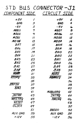
This is taken from the manual at http://www.bitsavers.org/pdf/ferguson/bigBoardII_Aug82.pdf. No further information is given in the manual.
Building a CP/M compatible system on perf-board
With a fresh success of building a computer from a kit, I decided to implement an existing design on perfboard, instead of drawing a design of my own right-away for breadboard building. Considering that the RC2014 is closely based on the work of Grant Searle, it was natural for me to take another design of his, and adapt to the 8-slot backplane: the "fully functional CP/M machine using only 9 chips" design.
I broke the design down to separate functional blocks, and built each as a separate card. By splitting the build into these distinct parts, I was able to build one card, and verify functionality of that card using the RC2014 before continuing to the next. All the cards were built on 100mm wide perfboard, using a direct soldered wire approach.
- RAM/ROM card
- SIO/2 serial IO card
- 8-bit IDE adapter for CF card
- CPU board with onboard Clock and Reset
- YM2149F sound card
I chose to make the RAM/ROM as a single combined card, because I did not want to split the ROM-disable function needed for CP/M up across two cards. It also allowed me to reduce the potential part count (by 1 IC). Because of the close relationship between the RC2014 design and the one I was implementing, I could simply use the ROM content from the RC2014 for verifying the ROM/RAM using the CPU and Serial I/O board from the kit.

Point-to-point wire soldered RAM/ROM card
Grant's CP/M design uses a different UART from the BASIC design. The BASIC design uses a 65B50, while the CP/M design uses a SIO/2. So this was the next card to be built. To verify this one, I burned a new ROM containing the "monitor" for the complete CP/M-design. This monitor also includes an 8k BASIC version, so it was easy to verify the SIO/2 board without having a CF-storage approach available.

Digital Out, RAM/ROM and SIO/2 cards installed
The original breadboard design page talks a bit about how to wire up a Compact Flash card, and how to hand-solder the SMD connector used for CF-cards. I did really not want to deal with that connector directly, and gambled on being able to use an IDE-to-CF adapter, considering the design really uses CF in 8-bit IDE mode anyway. My "IDE adapter" is basically a couple of OR-gates, an '138 address decoder, some resistors and a 40-pin male header connector. And it worked! With a short IDE cable between my "adapter" and a commercial IDECF-adapter, I was able to prep the CF card, load software onto it, and boot to a lovely "A>" prompt!

Possibly the simplest IDE adapter I could make
I could have rested here, but decided to whip up a new CPU board, as that, plus the clock generator, now was the only cards from the RC2014 kit that was in use. I integrated the clock, and also added an auto-reset onto the CPU card.
With these cards on the backplane, I now had a working Z80 based system, that I had needed to do some desgin-work for myself to adapt it to multiple cards. It was even a working CP/M system, with bonus ROM-based BASIC. To further verify that I did indeed have a CP/M compatible system, I grabbed a copy of Zork 1, I think it was from http://www.retroarchive.org/cpm/games/games.htm, and loaded it onto the CF-card using Grant's DOWNLOAD.COM utility. I believe any fully CP/M compatible system should have a copy of Zork 1 on it. And mine does, and it works 😀 I have used Zork as a demonstration of the system so much now, that my friends and colleagues have started to call my homebrew CP/M computers "the Zork machines" 😀

Zork I box art
The final card I built for the RC2014 bus, was a YM2149F synthesizer sound chip adapter. It required some fairly weird address decoding logic, so I spent quite a while on the design of this relatively simple card. After laying it out on perfboard and soldering up the wiring, I had a working sound card. I do believe I am starting to get a hang of this... What I still don't have as good a hang of, is large-scale assembly projects. So, I have tested the YM-card extensively from BASIC, and I have some general test-routines for it written in Assembly. But I have not made any proper songs using it, and I am quite far from implementing a Tracker or Player of any kind.
What I have used the system for, however, is getting to know how to code z80 Assembly for CP/M. It's a neat little operating system. A task as "small" as reading a file from disk has you digging quite deep into the system itself. As a result you end up with a very deep understanding of how the operating system internals work. And being such a small operating system, it is quite possible for a person to understand the entire operating system, after a reasonably short time studying it.
I created a final board for the system. By using a very cheap Chinese strip-board, I created a barebones version of the backplane. This freed up the RC2014 backplane to go back to being used with the original kit, and also made the computer a completely homebrew build. After this, the electronics part of the perfboard project was done. With such great results on the electronics side, I figured it deserved a nice place to live, and not become yet another stack of project parts in one of my bins of such. So I built a wooden cabinet for it, with some 3D printed parts to hold the cards in place. The case is made from beech wood, with an inlaid aluminium front.

My RC2014-based CP/M computer in a nice wooden case
This post is part of a series documenting my journey in making my own homebrew computer, the posts can be found on this link.