Adapters and addons to my 8-bit micro
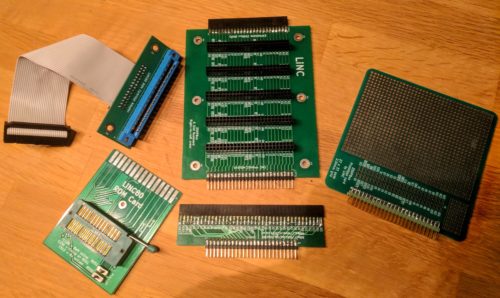
A collection of addon- and adapter cards
While testing my homebrew computer, I made some home-made addons, both in form of perf-board construction and home-etched PCB. I actually also made a connector-on-cable adapter, where I soldered the individual lines of a 30-pin ribbon cable onto an 805-series card-edge connector on one end, and because I failed to properly crimp an IDC connector on the other, I ended up soldering all 30 pins on that side as well. The other home-made adapters I made were: parallel input tester (perf), parallel output tester (perf), adapter from Z50Bus to RC2014 backplane (perf) and ROM Cartridge (PCB).
Considering how good the PCBs I got manufactured for the LiNC80 SBC1 itself, and how much effort went into making the Z50Bus-RC2014 adapter, I decided I wanted to get manufactured a set of support cards for the machine, and make it all look just as good. Additionally, having these support cards available would mean that I could have a small «ecosystem» of parts for future kit availability.
ROM Cartridge
The first card I designed was the ROM Cartridge PCB. The design I sent to manufacture for that was simply a slight tweak of the design I had already etched for testing, so it made sense to complete that first.
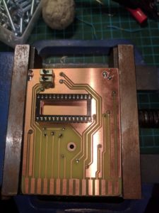 DIY etched ROM Cart |
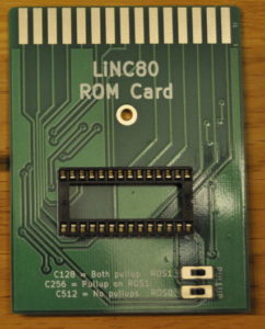 Manufactured ROM Cart PCB |
The card is designed to be large enough to comfortably insert and remove. It has a 28pin location for either a direct soldered or socketed ROM chip, and a central mounting hole for encased cartridges. The two two-position jumper locations allow for any ROM chip size between 16 and 64kByte, taking advantage of the LiNC80 ROM Bank select signals for ROM sizes above 16kByte. If the intended ROM application fits in a 4k or 8k chip, it’s naturally no problem to use chips of those sizes, as the pinout on the connector is JEDEC compliant.
Two jumpers are also on the board, making the choice of ROM chip size flexibility possible, and at the same time giving access to (and control over) the ROM bank select signals on my rom slot connector.
ROM Cartridge Slot
As I mentioned, I hand-soldered ribbon cable onto connectors to test the ROM Slot functionality of my design. Anyone who has tried soldering ribbon cable knows how much pain that is. To anyone who has not tried: avoid it if you can. So to spare anyone else from the unpleasant soldering task, I made up a simple passive IDC-to-Cardedge adapter.
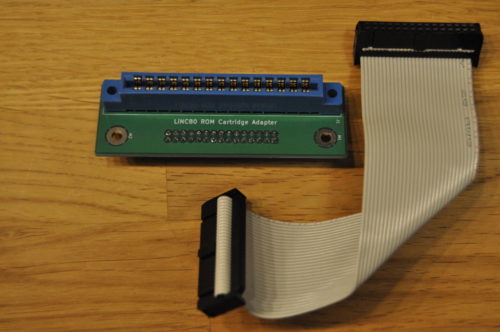
I decided to go with male header pins on the PCB, and use a ribbon cable with female IDC connector on both ends. Mounting IDC connectors can be easily done with a simple vise as a replacement for expensive pressing tools. A simple guide on how to do the vise approach can be found at https://startingelectronics.org/articles/IDC-ribbon-cable/
This is a purely passive adapter, with a pin-for-pin connection for all 30 pins. This means it can also be used as a general pinheader/IDC-to-cardedge adapter in addition to its intended use.
5 Slot Z50Bus
When I first started my design, and came up with the Z50Bus, I realized that I would have to make some kind of bus back-plane card. For this first iteration/version, I decided to make a purely passive one, without any bus buffering built in. I didn't even provide locations for decoupling capacitors, leaving the responsibility for those kinds of things to the expansion cards.
The back-plane has 5 standard slots. Connection to my computer on the right-hand side because the expansion connector on that board is on the left... On the left hand side of the back-plane is an extension header, meaning in theory, multiple cards can be added in a chain.
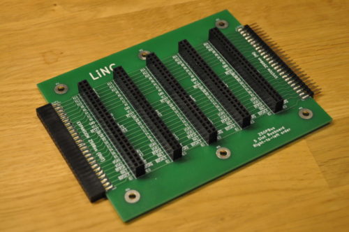
5-slot backplane
Speaking of chains. The Interrupt Chain signals IEI/IEO on this card are connected in a right-to-left order. This makes the first slot be on the right-hand side of the card, closest to the Z50Bus host.
Prototyping card
With a back-plane available, it would be nice to have some compatible expansions. Unfortunately, I hadn't made any of those yet. And I had quite early on realized that my choice of dual-row headers for the bus made prototyping more difficult than if i had gone for single-row. The natural step from this, was to make a made-to-fit prototyping perf-board!
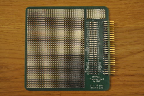
Prototyping card
My board provides a main prototyping area of 27 by 37 individual pads on a standard 2.54mm grid, plus an additional grid of 9 by 5 pads. The 50-pin bus connector is broken out on easily accessible connection points, providing two connecting pads per signal. I chose to make the board exactly 100x100mm. The real reason for this size is that most DIY-friendly board manufacturers have especially low prices for boards up to (including) just that size.
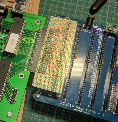
Adapter for RC2014
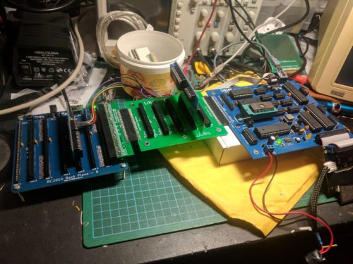
Because I already had built an RC2014 kit, as well as a couple of addons for that system, I felt it made sense to be able to test my expansion bus using those. i had after all designed the bus to be relatively compatible. During building and testing, I created a perf-board version of an adapter, with pin-to-pin wiring. This worked, but it was fragile. In the picture below, you can see this prototype connecting my Revision A computer to an 8-slot RC2014 backplane (not shown is that it works, and runs RC2014 ROM software off the backplane).
Because this is a trivial adapter, it was a simple design. I tried to compress it without making it DIY-unfriendly. As part of the design, I added pads allowing selection of horizontal or vertical mounting of the RC2014-side of things. On the Z50Bus side of things, I decided to use on-edge mounting of the header simply because I like that style.
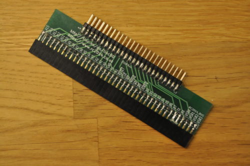
Bus-adapter card
I made a mistake in the design of this one. It's not a problem for most add-on cards, but it caused me problems when I tried to test the adapter. My mistake was to wire ALL signals for the simple RC2014 bus straight to the Z50Bus. Including the RX and TX lines. When I tried testing the MC68B50 serial card on the adapter, my system would seemingly not boot. I struggled for a while trying to figure that out, until I realized... The MC68B50 UART and the SIO/2 DUART were both connected to those lines. And both were trying to drive the lines! So my system was booting, but my terminal could not see that, and could not talk to the UART either. By cutting the two traces for RX and TX respectively, I had no problems with any of the modules I had to test. Even running a «Full monty» RC2014 on the RC2014 backplane, using the LiNC80 as just CPU and RAM worked without any issues.
Creative combinations of back-planes, adapters and modules
I may do an update of this board, with jumpers or solder-pads on those two lines, but as long as the user is aware that adding multiple UART chips on the same lines cause problems, I think the current version will work fine.
Before I add my closing line... I am really gearing toward making kits! They aren't quite available for sale yet, but the product presentations and documentation is coming up on my business-site! To start navigation directly from the LiNC80-pages, go to http://linc.no/go/linc80. To see what else I have on offer, see http://linc.no/products, where you also can find the more "official home" of the Z50Bus specification and accessories
This post is part of a series documenting my journey in making my own homebrew computer, the posts can be found on this link.