Z50Bus – A compact expansion bus for 8-bit microcomputers
Note!
The new, more official page for the Z50Bus is located at http://linc.no/products/z50bus
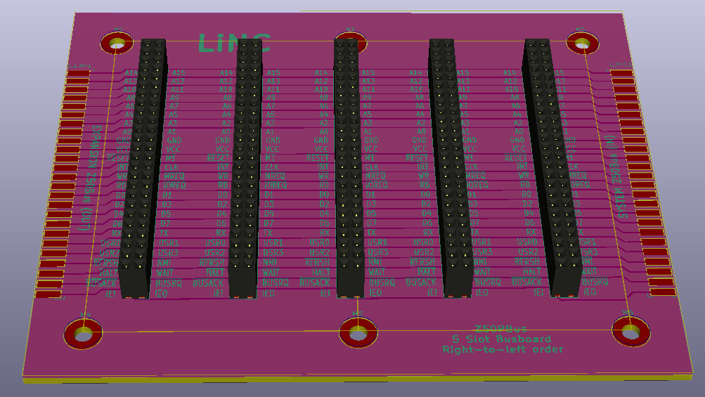
A 5 "slot" Z50Bus backplane
The Z50Bus is a suggestion for a system expansion bus for 8-bit microcomputers. First, a little background. It came into existence early in my design phase of my own homebrew computer. As such it is a new bus layout, and my personal needs is reflected in its layout. I wanted an expandable system, I wanted it to have a documented bus layout to allow others to design around it, the bus should be electrically simple, and require few logical components to implement. To satisfy the criteria of being simple and require few components, the layout needed to be close to the CPU I intended to use. As a result of that, the bus is closely tied to the CPU signals of the Zilog Z80 CPU. I investigated using an existing bus layout. The standardized bus layouts that I found to be relevant were S100[1][2] and STD80[1][2] or the 56-pin variant of the STD bus, as used by the Ferguson Big Board II shown at the bottom of this post. In my opinion, using any of these would require more complexity than I wanted. Following the actual standards would also be required, which would require the use of 100-, 80- or 56-pin edge connectors, and including voltage levels that seem weird in modern systems. Most of +8V, +16V and -16V, +12V and -12V would need to be included. I also looked to the popular homebrew kit system RC2014. Its bus layout is very simple, and with a SIL-like connector, it's very easy to make prototypes for the system. What I don't like about the bus, is that the standard version does not implement all useful CPU signals, and the physical rigidity of the connectors is weak. So, I wanted to use a pin-header based connection that is more rigid than a single row, and at the same time let the width of the physical connection be fairly small.
The name of the Z50Bus comes from being originally designed to use a 50-pin connector to integrate a system around a Z80 CPU. Being a simple bus specification, it is possible to use/integrate it with other 8-bit CPUs using some glue logic. One such example is shown later, for using a 65C02 CPU.
Signal levels and descriptions
Signal levels are 5V Single Ended, with HC TTL levels expected. So, each signal uses a single line, and an active high signal will have a High at 3.5V - 5V, and a Low state at 0-1V. The 5V and GND lines are the only supply voltages on the bus. System implementations should make sure these are noise-free, well decoupled, and dimensioned for the system current draw.
The bus uses a double-row connector scheme, with the following pin layout
| Pin | Signal name | Pin | |
| 1 | A15 | A14 | 2 |
| 3 | A13 | A12 | 4 |
| 5 | A11 | A10 | 6 |
| 7 | A9 | A8 | 8 |
| 9 | A7 | A6 | 10 |
| 11 | A5 | A4 | 12 |
| 13 | A3 | A2 | 14 |
| 15 | A1 | A0 | 16 |
| 17 | Gnd | Gnd | 18 |
| 19 | 5V | 5V | 20 |
| 21 | /M1 | /Rst | 22 |
| 23 | Clock | /Int | 24 |
| 25 | /Mreq | /WR | 26 |
| 27 | /IOreq | /RD | 28 |
| 29 | D1 | D0 | 30 |
| 31 | D3 | D2 | 32 |
| 33 | D5 | D4 | 34 |
| 35 | D7 | D6 | 36 |
| 37 | Tx | Rx | 38 |
| 39 | Usr1 | Usr0 | 40 |
| 41 | Usr3 | Usr2 | 42 |
| 43 | /NMI | /Refresh | 44 |
| 45 | /Wait | /Halt | 46 |
| 47 | /BusRQ | /BusACK | 48 |
| 49 | IEO (*) | IEI (*) | 50 |
Female bus - Male card
* Note that IEO/IEI forms an Interrupt Enable Chain, where the IEO of a higher priority card needs to connect to a lower priority card. This means a bus board needs to connect IEO of one "slot" to the IEI of the next. It also means cards need to be present "in order", or empty slots need IEI/IEO jumpered for interrupts to work.
This layout of the signals is relatively simple to lay out for both CPU and expansion cards. Additionally, it is easily "unfolded" onto a single-row implementation, where using the first 42 pins mapped onto a 1x40 connector gives full compatibility with the bus layout of the RC2014 compatible ecosystem.
The on-bus signals function/description closely follow Z80 CPU signals, with a few extra signals inspired/compatible with the RC2014 signal set:
| D7..D0 | Data bus lines |
| Clock | System / CPU Clock (Phi2Out for 6502) |
| /Rst | System Reset, Active Low |
| /Mreq | Memory Request, Active Low, CPU Output |
| /IOreq | IO Request, Active Low, CPU Output (synthetic for 6502) |
| /WR | Write, Active Low, CPU Output |
| /RD | Read, Active Low, CPU Output |
| /M1 |
Machine Cycle One, Active Low, CPU Output (M1+IORQ active indicates INTAck. May use SYNC on 6502)
|
| /Int |
Interrupt, Active Low, CPU Input, device requests interrupt by pulling INT low.
|
| /NMI |
Non Maskable Interrupt, Active Low, CPU Input, device requests interrupt by pulling INT low.
|
| /Wait |
Wait, Active Low, CPU Input, used to hold the CPU for wait states (can integrate RDY for 6502)
|
| /Halt |
Halted, Active Low, CPU Output, indicates that the CPU is in WAIT FOR INTERRUPT state (HALT or WAI instructions)
|
| /BusRQ |
Bus Request, Active Low, CPU Input, used to request bus control, i.e. for DMA
|
| /BusACK |
Bus Acknowledge, Active Low, CPU Output, indicates that a BusRQ is accepted, and that CPU signals are high-Z
|
| /Refresh |
DRAM Refresh cycle, Active Low, CPU Output. When Refresh and Mreq are active, a DRAM refresh can be done
|
| IEO (*) |
Interrupt Enable Out, Active High output from one expansion card to next expansion.
|
| IEI (*) |
Interrupt Enable In, Active High input to expansion from previous expansion card or system/CPU board
|
| Tx / Rx | System internal TTL Serial |
| Usr0..Usr3 |
User Definable pins (USER1...4 on RC2014, note numbering difference)
|
The signal layout for Z50Bus is simplistic, and makes very little attempt at being a signal balanced and noise cancelling bus design. The bus specification itself does not indicate if a system should use buffered bus or buffered expansions (or be raw CPU signals).
Mechanical implementation and suggestions
The standard bus connector to be used, is 50-pin dual-row header pin and socket, with 2.54mm pin pitch. For expansion cards that plug into a busboard, a Male pin header with nominal 6mm pin length should be used ("standard" header, sometimes called 11mm). The bus-side connector should be a Female PCB Header Socket, with nominal 8.5mm height.
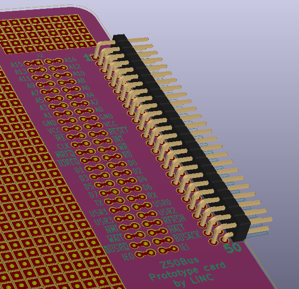
The suggested arrangement for expansion cards is to use a Right angled connector. For orientation, an expansion card laid out so the connector is on the right hand side should have pins 1 and 2 as the top pair, 49 & 50 the bottom, and the connector on the component side.
Mechanical layout is not strictly bound by the bus layout and design, but to allow for card supports, the following suggestions apply. On an expansion card, the center pair of pins (and thus the center of the connector) should be located 50mm from the edge closest to the connector pins 1 & 2. The card should leave space for a support raiser going 2.5mm in from the edge closest to pins 1 & 2, extending 20mm along that edge.
 Connector on expansion card for Z50Bus |
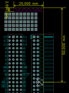 Position of connector |
For connectors used to connect a system board and expansion or bus-board, the suggested arrangement is to use straight connectors placed on-edge, female connector on the system board (main bus) side, and male on the expansion (exp bus) side. This allows the main-bus card and the exp-bus card to lie in the same plane, without requiring expensive right-angle 2x25 socket headers.
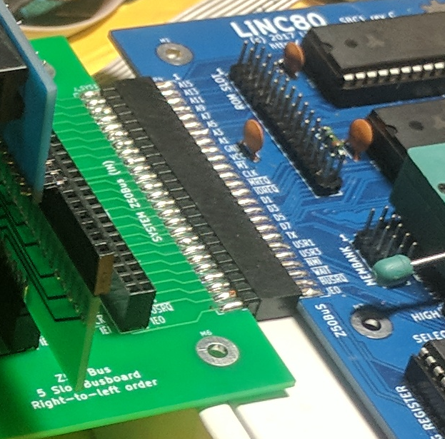
Example of on-edge connectors for joining a system board (right, female connector) to an expansion bus board (left, male connector)
Using the Z50Bus with the 6502
Being a bus for 8-bit microcomputers designed after 2016, the number of potential CPU's relevant for new designs is limited. Currently only the Z80-family and the 65x02 family of CPU's have parts still in production. Because of this, only a 65x02 adaption of the bus is suggested here.
Some of the Z80-style signals need to be synthesized. 65x02 uses memory mapped IO, so the IOReq signal needs to be generated by the CPU card/system when a request is made to the 65x02 IO address space selected for the system. The Mreq signal will then be a simple invert of the IOReq signal. An equivalent function of the WAIT and HALT signals may be found on the 65x02 RDY line. A diode split of the function may be appropriate. The SYNC signal can be adapted for the M1 signal function, if the INTAck feature is considered in the implementation.
| 65C02S signal | Z50Bus | Z80 signal | RC2014 |
| *SYNC | M1 | M1 | N/A |
| (generated) | MREQ | MREQ | MREQ |
| (generated) | IOREQ | IOREQ | IOREQ |
| *R/W | RD | RD | RD |
| R/W | WR | WR | WR |
| N/A | RFSH | RFSH | N/A |
| (RDY) | HALT | HALT | N/A |
| (RDY) | WAIT | WAIT | N/A |
| INT | INT | INT | INT |
| NMI | NMI | NMI | NMI |
| RES | RST | RESET | RST |
| BE (Jump) | BUSRQ | BUSRQ | N/A |
| N/A | BUSAK | BUSAK | N/A |
| PH2 (clk out) | CLK | CLK | CLK |
| A0-A15* | A0-A15 | A0-A15 | A0-A15 |
| D0-D7 | D0-D7 | D0-D7 | D0-D7 |
| ML (Jump) | USR0 | ||
| VP (Jump to GND) | |||
| SO | USR1 |
There exists a 65c02 CPU card for the RC2014 system, this should be seen as the reference implementation when adapted to Z50Bus layout for the basic signals. See http://ancientcomputing.blogspot.no/2017/05/a-6502-cpu-for-rc2014-part-1.html. It is suggested that 65x02 based systems using the Z50Bus indicate clearly that not all expansion cards designed for a Z80 native Z50Bus system will be compatible.
56-pin STD Bus
For reference, I choose to include an image of the pinout/layout of the STD bus as it was used on the Ferguson Big Board II. The reason for including it, is that it was not easy to locate this information when I was researching, and I want to preserve this information. Note that the standardized STD interfaces use 80-pin card edge connectors, while the Big Board II used a 56 pin pin-header + header socket format with 2.54mm spacing
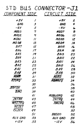
This is taken from the manual at http://www.bitsavers.org/pdf/ferguson/bigBoardII_Aug82.pdf. No further information is given in the manual.