The birth of my Z80 computer design, the LiNC80 SBC1
I originally started my adventure of homebrew computer building thinking I'd build a relatively simple system. This thought soon changed, as I outlined in the "scribbling ideas" post. The main reason for daring to be more ambitious was basically that with a good base design like the "Fully functional Z80 CP/M machine using only 9 chips" from Grant Searle, and a bit of experience, it seemed to be well within reach! Grabbing the list from the "scribbling ideas" post, my top-level selection of features ended up with this:
- Z80 CPU
- Zilog SIO/2 serial port controller with dual serial ports
- Zilog CTC for four channels of Counter/Timer, 2 of them dedicated to the SIO/2
- Zilog PIO for two Parallel ports
- Expandable system through Z50Bus
- Memory map designed to allow for graphics expansion
- CP/M compatibility
- ROM part of memory from address $0000 disable-able (needed for CP/M and more)
- For fun, a dedicated ROM Cartridge connector
- Z80 Interrupt Mode 2 in the core
- Compatibility with software from Grant Searle (for easy system bring-up)
In addition to that list, I set a limitation of component selection, all active components had to be currently active parts available as new from manufacturer. I also wanted to use static RAM, and have 64KByte of it in DIP packages, so the design uses two 32kx8 SRAM ICs.
I'm really not much of a software-guy. I can program, and I know my way around assembler code, but I am most definitely not one of those guys that can code a ROM Monitor in an evening. Being able to re-use existing software helps me get my system up and running. The fact that Grants software works well, on a system that can run an operating system I want to use, means it would be silly of me to not take advantage of that. Because that existing software uses IM2, I would have to use IM2 as well, or commit to some serious software redesign. Besides, I wanted to try out IM2 more because I think it's cool. My desire to run CP/M also dictates the need to have a way to disable (or move) ROM out from address $0000 of the memory-map.
The "dependency effect" of using existing code also makes itself visible in hardware I/O address selection. To avoid changing too much code, it makes sense for me to place the SIO/2, ROM-disable and CF-disk I/O addresses on the same addresses used in Grant's design. I also liked his approach of using a 74LS138 for decoding, so I stuck with that approach, and selected "remaining" decode outputs for use with the CTC and PIO. The decoding logic ends up "eating up" 8 I/O addresses for each "on-board device", so 40 I/O addresses in the ranges 0x00 to 0x1F and 0x38 to 0x3F are locked. Somewhat expensive in terms of resources, but it allows for a simple construction with few parts. Besides, all addresses from 0x40 and up to 0xFF are still available for expansions.
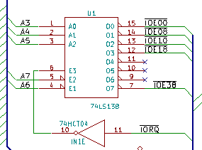
I/O address decoding for on-board devices
As listed, I wanted to be able to use software-controllable bit/baud rates on the serial ports. To be able to do that I chose to include the Z80CTC, a counter/timer controller, to drive the SIO. But I wasn't quite sure about my Z80 assembly skills yet, so I decided to include a jumper-selector to select SIO-clock to be CPU clock or CTC. That way, I could select CPU-clock for booting unmodified code from Grant, and then switch to CTC-clock once I knew how to do that.
My first major divergence from the base design came as a result of my desire to have a memory map designed for graphics. Being able to combine that with the option of running code other people has made for Grant's design, meant that I had to include some kind of bank-switching. The design already included a very basic form of bank-switching: Grant has designed the "disable ROM" feature as a simple RS-latch that bank-switches the lower 16k between ROM and RAM. To switch from the ROM bank to the RAM bank, a write to address 0x38 needs to be done. In his design, the bank switch is triggered by an I/O write to the correct address, and the data is not used for anything. I examined the source code and found out that even if you only need to write something to the address, his code actually writes the value 0x01. Based on that, I decided that my "memory management" for bank-switching could be done using some kind of register, placed at 0x38, as long as the lowest bit of the register was used for enabling/disabling ROM. This would additionally give me the option of switching ROM back in, in contrast to Grants design where only a system reset would bring ROM back into active memory.
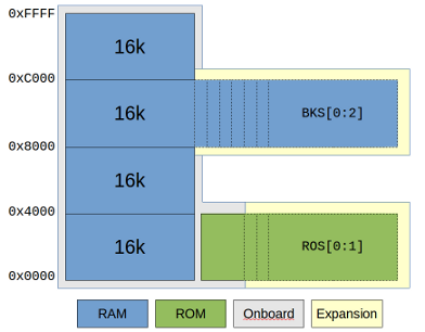
Armed with a general idea on how I could do bank-switching, I started looking at how I could make a memory map that worked with both CP/M and graphics. Because CP/M needs to have its BIOS and BDOS placed in a predictable, always available location in memory, and it expects RAM in the bottom of memory, my options were a bit limited. On top of that, I wanted to at least start with existing software, and the software I had available expected to be able to stuff BDOS, BIOS, ISRs and stack in the top 8-16k of memory. That made me decide to use a fairly odd and uncommon memory map. I decided that the second-top-most 16k would be the "window" for bank-switching. Basically, bottom 16k is switchable RAM/ROM, second 16k is always on-board RAM, third 16k is switchable memory defaulting to on-board RAM, and fourth and final 16k is always on-board RAM.
With the general memory map laid out, I turned my attention back to that register I talked about earlier. I decided I'd go for the simplest approach I could think of, one that I had used to implement a simple digital-out solution for the RC2014 computer. By using a 74LS273, I could get a very simple 8-bit write-only register. To quote the data sheet: «The SN54/74LS273 is a high-speed 8-Bit Register. The register consists of eight D-Type Flip-Flops with a Common Clock and an asynchronous active LOW Master Reset.». Placing one of those on I/O address 0x38, using IO Write as clock input and the data bus as D-inputs, I could use the outputs to perform bank switch selection. Using the system RESET signal for the '273s Master Reset, the system would always reset to a predictable state. And by using the lowest bit to control ROM disabling, I had compatibility with the existing code from Grant! With seven bits still available, I decided to use three bits for RAM bank select. This would let me simply use another LS138 to select one of eight RAM banks, and by using "location 000" for the on-board RAM, things should boot nicely.
I selected to use one bit of the "register" to control Interrupt Enable Input of onboard devices. This would let me "lock" interrupts to an IM2 disabled state, a feature I thought would be handy to have on top of the Interrupt Enable / Disable Interrupt instructions of the CPU. This left me with a few bits left over. In my scribbling, the idea of having a ROM cartridge for fun and experimentation had been added. I quickly added to that idea, by using two of the bits as "off-board ROM bank selects". That would allow a ROM cartridge to have four 16k banks! Which by the way matches nicely with a standard 64Kbyte ROM chip size.
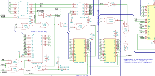
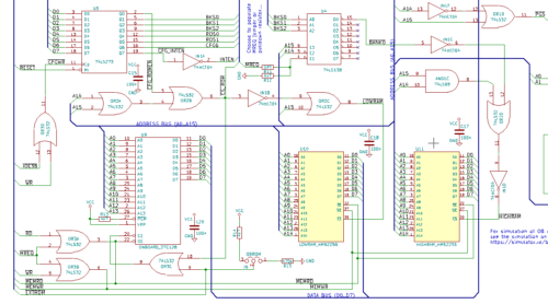
With memory map idea fleshed out, I had to figure out a way to make the memory decode and interfacing work. I ended up finding a cool tool at https://simulator.io/ that allows for on-line simulation of digital logic. Using first a set of logic tables, I assembled an idea, and implemented it on simulator.io first, before adding it to my design. You can see and play with the result at https://simulator.io/board/RoLQ8QDEei/2. Confident that I had a memory layout that could work, and a decode logic that seemed to make sense, I started the actual design. The resulting memory interfacing logic took quite a bit more glue logic than Grants simple design, but I think it came out quite nice.
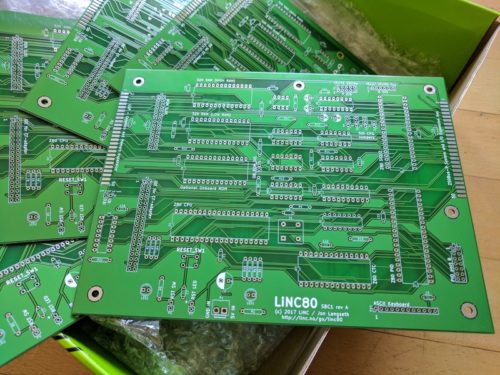
The overall schematic I had in KiCAD was at this point starting to get large and complex. Thinking back at my issues with flaky breadboards, I was starting to dread building something as complex as this on either wonky breadboards, or on a very large perf-board. It would be doable, but the thought of debugging soldered point-to-point or bad breadboard connectors didn't really sound tempting. At the same time, I was still learning to use KiCAD for a somewhat large design, and I more or less accidentally started laying out a PCB. Combining manual parts layout, a bit of manual routing and experimentation with freerouting, I suddenly had a board layout that looked decent. So I took a gamble, and simply sent off some money and a few gerber files to seeed studio. Not a full week later, I received a box containing five fine looking PCBs.
This board was designed with all the bullet points from the design list. There's SIO/2, CTC and PIO devices, an IDE connector, and on the right side, a Z50Bus expansion bus. Additionally, I created a different version of an expansion connector on the left side that included all the decoded bank-switching lines (but not all CPU-signals, to keep it on a 50-pin connector).
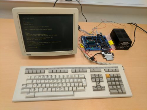
Seeing how nice my PCB looked, I got to work assembling it. I soldered in passives, added sockets for IC's, and completed all soldering. After some experience with how much rosin flux can affect a complex logic circuit, I cleaned the board thoroughly before adding any of the semiconductor components. Finally, I hooked up serial ports and applied power.
Nothing happened.
Or, well, something happened. The board started drawing current, and it was well within expected range. So it would seem that the reason for it not working wasn't a dead short or a major defect. It had to be some kind of logic design flaw. I got a hold of a cheap logic analyzer to try to figure out what was wrong, but I couldn't get the analyzer to trig properly on the T1-T3 multi-clock-per-instruction that the Z80 has. I shelved the project in frustration for a while. After some months of not working on it, I brought it back out, and started poking around. After seeing some weird behavior, and a bit of "almost working" if I removed both the 'LS138 and the 'LS273, I figured something was weird with the I/O addressing. On examining the schematic in detail, I realized I had made two really silly mistakes.
The I/O address decoder was always active, doing its decoding even on Memory operations and even on the built-in DRAM refresh. Next, the 'LS273 that I was using as my "configuration register" only used the I/O address decode signal as its "Write" signal! These two problems together meant that the contents of the "register" was constantly changing. I'm not surprised that the code in ROM was less than happy about getting bank-switched out half-way through an instruction... Fortunately, I had spare logic elements in the glue logic IC's. This allowed me to fix the problems using bodge-wires and cut traces on the back of the PCB. The same evening I discovered my errors the system started doing what I had intended, and I had working CP/M on my slick-looking homebrew PCB.
I decided it would be best to fix the mistakes in my schematic, so I went back to KiCAD and implemented the changes that I had made on the board. I swapped some gate selection around to make the glue logic easier to route. While I was looking at the routing issues, I had a long think about the whole "two expansion ports, one for system and one for graphics". In the end, I decided it did not really make sense. I could put all the memory/bankswitch and graphics-only signals on a much smaller header connector, and use a cable to a standard Z50Bus expansion card. That would mean only one expansion connector would be needed. This in turn would lead to much simpler routing of the board, and the board could be physically smaller, reducing cost.
Reducing cost may sound weird. After all, this is my homebrew design, and I already had a working computer in front of me. But at this point, I was seriously considering making this a kit. And if I was to sell any of these, making the cost of the PCB go down would be a good plan. So, the changes were implemented, I did a new layout, and sent it off to seeed for fabrication. 10 days later I got a new batch of boards that I fairly quickly assembled. I transplanted all ICs from the previous build over, and tested it.
And it did not work. ARGH!
Back to the schematic, I found ONE silly mistake. While I was redesigning, I had done some changes to the schematic around the SIO/2 chip, and while doing that, I had swapped the address lines A0 and A1 by accident. That meant that the Control and Data addresses had become swapped. A quick cut-and-solder on the PCB swapped those back, and the computer came to life! I set to work writing code to test the other on-board devices that aren't on Grants design. I got the CTC to clock and generate interrupts, and I got the PIO to work as Byte-out, Byte-in, and bit-in-out. But no matter what I did, I could not get the PIO to generate interrupts.
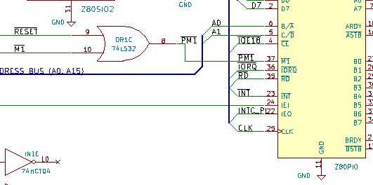
It turns out, the PIO interrupt signal is gated by its M1 input. And, because the PIO actually has one pin less than it needs, Zilog chose to make a multiplexed M1+Reset function on the M1 pin. And in my design, I had thought "M1 input is active if either CPU M1 is active OR if system Reset is active". So I had put an OR gate there. There's one problem with this. Both Reset and M1 are ACTIVE LOW signals. And to make an "or" function for active low signals, you need to use an "and" gate! Long live boolean logic and active low signals. Who would have thought OR to be different from AND in boolean logic... I managed to finagle this by more bodging, and eventually I had a fully working computer, where all on-board devices worked.
Considering the amount of self-inflicted troubles I had experienced so far, I decided to test the expansion bus and the ROM cartridge connections before fixing my schematic again. To my relief, both of those worked without problems. I was able to use a ROM cartridge with ROM bank select, and was even able to use the RC2014 backplane to test using off-board memory and off-board devices.
During the testing of the ROM cartridge solution, I discovered that the rule of only using parts still in production had been violated on my design. I had based the on-board ROM circuit on a 16Kx8 EPROM, the 27c128. That ROM chip is not available, and neither is it's EEPROM-version, the 28c128. Fortunately for me, the bigger AT28C256 is still in production, and very close to pin compatible. I revised the schematic and board to include two jumpers for on-board ROM allowing either tied VCC signal for 'c128-devices, or use of the ROM-select lines. This makes it possible to select between 'c128, 'c256 and 'c512 ROM chips (16k, 32k and 64k), and even use of bank switching for on-board ROM. The physical placement of the jumpers was done so a ZIF-socket would fit (it's tight, but it fits), just because I could.
Considering the errors in this revision B of the board, I made corrections, and created revision C. This board now carries my official name for my homebrew computer design as it stands today: the LiNC80 Single Board Computer 1 Rev C. Considering it is an expandable board, with no on-board graphics, it may seem strange that I call it an SBC. Before the arrival of a heap of BeagleBoard and Raspberry Pi like devices, it was usual to call a PCB that implemented a fully working embeddable computer an SBC, and it was unusual for SBCs to have local graphics, but not unusual for them to have expansion/interface connectors.
Revision C of the board still has a minor issue, but none that makes a real difference to a system user that is aware of it. The only significant problem I see at the moment, is related to how the two serial ports behave on RTS/CTS signals if one of the ports is left unconnected. On the board, there is a jumper that selects between honoring incoming CTS (RTS from other host), or tying it to Gnd. If unconnected and not tied to Gnd, the SIOA tends to lock up the second serial port SIOB. On the other hand, if SIOA is connected, but SIOB is left unconnected, random characters may get generated if the CTS input is floating. The solution is to jumper the unused CTS signal to "disabled" for an unconnected SIO port.
This post is part of a series documenting my journey in making my own homebrew computer, the posts can be found on this link. Stay tuned for more posts in this series. The next will probably be about the various adapter cards I have planned/made.
Note! I am gearing toward making kits available!
The product description pages for the kit starts off at http://linc.no/products/linc80-sbc1/
The new, more official page for the Z50Bus is located at http://linc.no/products/z50bus



February 23rd, 2018 - 07:56
interesting design I would like a PCB or kit when available I also started with the great RC2014 and have two up and running but want to expand upon that with a nice Z80 design to play with
February 25th, 2018 - 23:35
If you are interested in a PCB or kit, please stay tuned, I’m working on it 🙂
June 14th, 2018 - 13:36
I should note here that PCB’s and kits are available, see links added to the original article 🙂
June 14th, 2018 - 07:23
Can it run Fuzix? (8-bit unixish)
http://fuzix.org/
June 14th, 2018 - 13:35
Without modifications, no. The onboard ROM provisions are far from the needs of Fuzix, and the banking approach is not Fuzix-friendly. If one were to remove RAM and ROM from the board, and make an expansion card with the needed ROM+RAM features, it’s possible, but at that point it would make more sense to do a complete new build, or to start from an RC2014.