Adapters and addons to my 8-bit micro
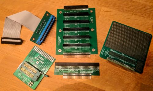
A collection of addon- and adapter cards
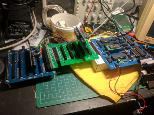
While testing my homebrew computer, I made some home-made addons, both in form of perf-board construction and home-etched PCB. I actually also made a connector-on-cable adapter, where I soldered the individual lines of a 30-pin ribbon cable onto an 805-series card-edge connector on one end, and because I failed to properly crimp an IDC connector on the other, I ended up soldering all 30 pins on that side as well. The other home-made adapters I made were: parallel input tester (perf), parallel output tester (perf), adapter from Z50Bus to RC2014 backplane (perf) and ROM Cartridge (PCB).
Considering how good the PCBs I got manufactured for the LiNC80 SBC1 itself, and how much effort went into making the Z50Bus-RC2014 adapter, I decided I wanted to get manufactured a set of support cards for the machine, and make it all look just as good. Additionally, having these support cards available would mean that I could have a small «ecosystem» of parts for future kit availability.
ROM Cartridge
The first card I designed was the ROM Cartridge PCB. The design I sent to manufacture for that was simply a slight tweak of the design I had already etched for testing, so it made sense to complete that first.
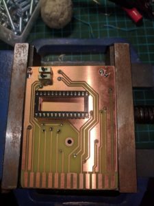 DIY etched ROM Cart |
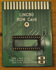 Manufactured ROM Cart PCB |
The card is designed to be large enough to comfortably insert and remove. It has a 28pin location for either a direct soldered or socketed ROM chip, and a central mounting hole for encased cartridges. The two two-position jumper locations allow for any ROM chip size between 16 and 64kByte, taking advantage of the LiNC80 ROM Bank select signals for ROM sizes above 16kByte. If the intended ROM application fits in a 4k or 8k chip, it’s naturally no problem to use chips of those sizes, as the pinout on the connector is JEDEC compliant.
Two jumpers are also on the board, making the choice of ROM chip size flexibility possible, and at the same time giving access to (and control over) the ROM bank select signals on my rom slot connector.
ROM Cartridge Slot
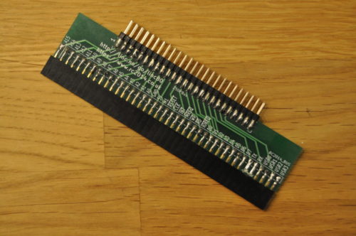
As I mentioned, I hand-soldered ribbon cable onto connectors to test the ROM Slot functionality of my design. Anyone who has tried soldering ribbon cable knows how much pain that is. To anyone who has not tried: avoid it if you can. So to spare anyone else from the unpleasant soldering task, I made up a simple passive IDC-to-Cardedge adapter.
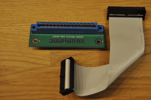
I decided to go with male header pins on the PCB, and use a ribbon cable with female IDC connector on both ends. Mounting IDC connectors can be easily done with a simple vise as a replacement for expensive pressing tools. A simple guide on how to do the vise approach can be found at https://startingelectronics.org/articles/IDC-ribbon-cable/
This is a purely passive adapter, with a pin-for-pin connection for all 30 pins. This means it can also be used as a general pinheader/IDC-to-cardedge adapter in addition to its intended use.
5 Slot Z50Bus
When I first started my design, and came up with the Z50Bus, I realized that I would have to make some kind of bus back-plane card. For this first iteration/version, I decided to make a purely passive one, without any bus buffering built in. I didn't even provide locations for decoupling capacitors, leaving the responsibility for those kinds of things to the expansion cards.
The back-plane has 5 standard slots. Connection to my computer on the right-hand side because the expansion connector on that board is on the left... On the left hand side of the back-plane is an extension header, meaning in theory, multiple cards can be added in a chain.
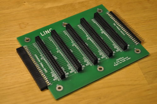
5-slot backplane
Speaking of chains. The Interrupt Chain signals IEI/IEO on this card are connected in a right-to-left order. This makes the first slot be on the right-hand side of the card, closest to the Z50Bus host.
Prototyping card
With a back-plane available, it would be nice to have some compatible expansions. Unfortunately, I hadn't made any of those yet. And I had quite early on realized that my choice of dual-row headers for the bus made prototyping more difficult than if i had gone for single-row. The natural step from this, was to make a made-to-fit prototyping perf-board!
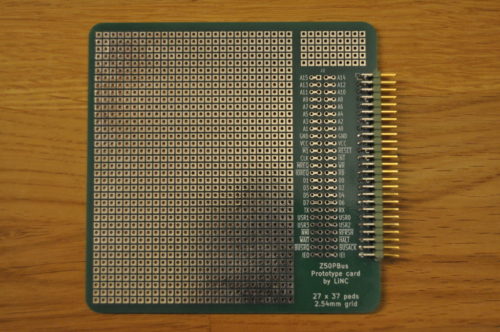
Prototyping card
My board provides a main prototyping area of 27 by 37 individual pads on a standard 2.54mm grid, plus an additional grid of 9 by 5 pads. The 50-pin bus connector is broken out on easily accessible connection points, providing two connecting pads per signal. I chose to make the board exactly 100x100mm. The real reason for this size is that most DIY-friendly board manufacturers have especially low prices for boards up to (including) just that size.
Adapter for RC2014
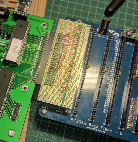
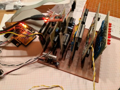
Because I already had built an RC2014 kit, as well as a couple of addons for that system, I felt it made sense to be able to test my expansion bus using those. i had after all designed the bus to be relatively compatible. During building and testing, I created a perf-board version of an adapter, with pin-to-pin wiring. This worked, but it was fragile. In the picture below, you can see this prototype connecting my Revision A computer to an 8-slot RC2014 backplane (not shown is that it works, and runs RC2014 ROM software off the backplane).
Because this is a trivial adapter, it was a simple design. I tried to compress it without making it DIY-unfriendly. As part of the design, I added pads allowing selection of horizontal or vertical mounting of the RC2014-side of things. On the Z50Bus side of things, I decided to use on-edge mounting of the header simply because I like that style.
Bus-adapter card
I made a mistake in the design of this one. It's not a problem for most add-on cards, but it caused me problems when I tried to test the adapter. My mistake was to wire ALL signals for the simple RC2014 bus straight to the Z50Bus. Including the RX and TX lines. When I tried testing the MC68B50 serial card on the adapter, my system would seemingly not boot. I struggled for a while trying to figure that out, until I realized... The MC68B50 UART and the SIO/2 DUART were both connected to those lines. And both were trying to drive the lines! So my system was booting, but my terminal could not see that, and could not talk to the UART either. By cutting the two traces for RX and TX respectively, I had no problems with any of the modules I had to test. Even running a «Full monty» RC2014 on the RC2014 backplane, using the LiNC80 as just CPU and RAM worked without any issues.
Creative combinations of back-planes, adapters and modules
I may do an update of this board, with jumpers or solder-pads on those two lines, but as long as the user is aware that adding multiple UART chips on the same lines cause problems, I think the current version will work fine.
Before I add my closing line... I am really gearing toward making kits! They aren't quite available for sale yet, but the product presentations and documentation is coming up on my business-site! To start navigation directly from the LiNC80-pages, go to http://linc.no/go/linc80. To see what else I have on offer, see http://linc.no/products, where you also can find the more "official home" of the Z50Bus specification and accessories
This post is part of a series documenting my journey in making my own homebrew computer, the posts can be found on this link.
The birth of my Z80 computer design, the LiNC80 SBC1
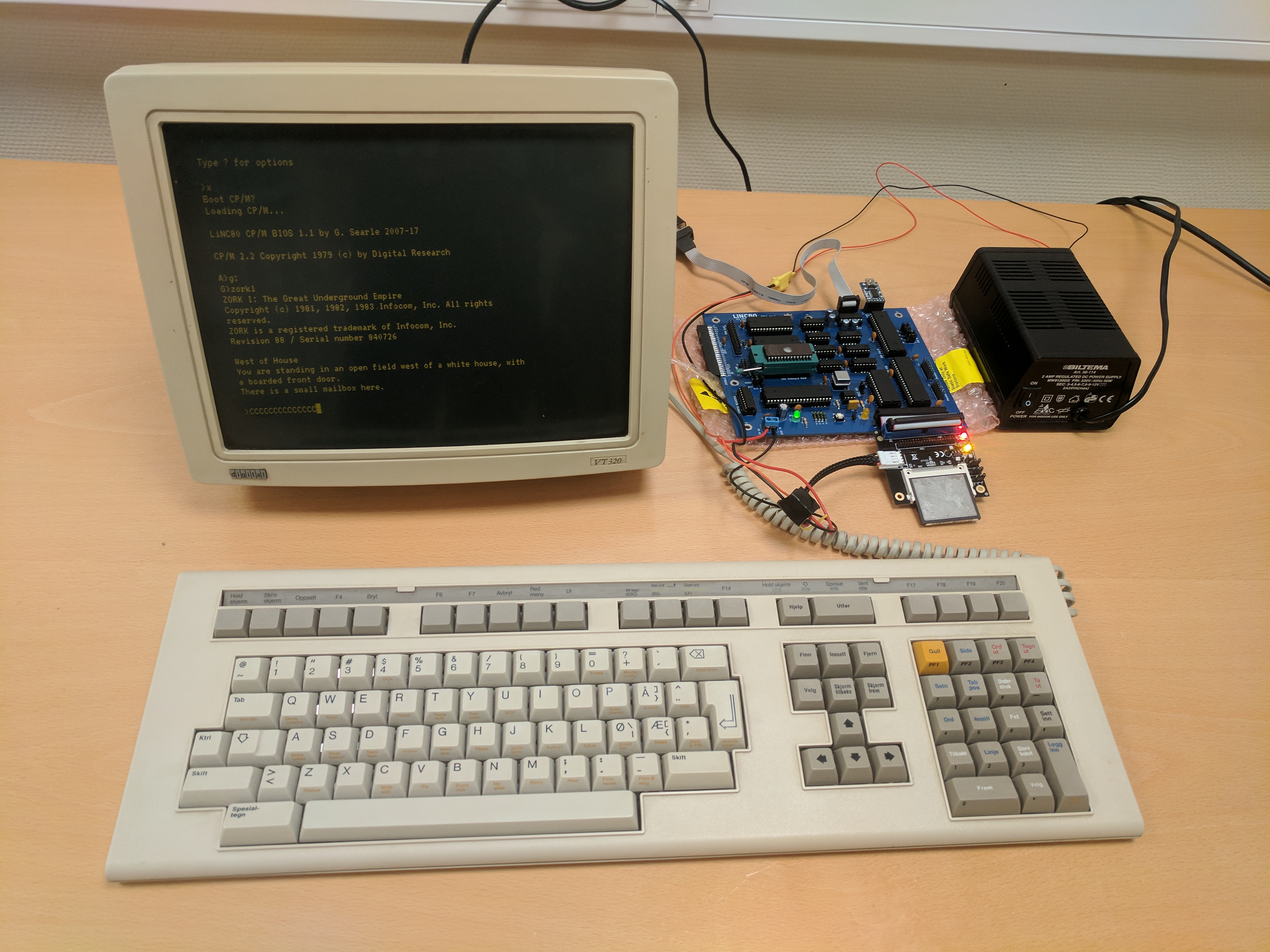
LiNC80 SBC1 Rev C running Zork I under CP/M, using DEC VT320 as serial terminal
I originally started my adventure of homebrew computer building thinking I'd build a relatively simple system. This thought soon changed, as I outlined in the "scribbling ideas" post. The main reason for daring to be more ambitious was basically that with a good base design like the "Fully functional Z80 CP/M machine using only 9 chips" from Grant Searle, and a bit of experience, it seemed to be well within reach! Grabbing the list from the "scribbling ideas" post, my top-level selection of features ended up with this:
- Z80 CPU
- Zilog SIO/2 serial port controller with dual serial ports
- Zilog CTC for four channels of Counter/Timer, 2 of them dedicated to the SIO/2
- Zilog PIO for two Parallel ports
- Expandable system through Z50Bus
- Memory map designed to allow for graphics expansion
- CP/M compatibility
- ROM part of memory from address $0000 disable-able (needed for CP/M and more)
- For fun, a dedicated ROM Cartridge connector
- Z80 Interrupt Mode 2 in the core
- Compatibility with software from Grant Searle (for easy system bring-up)
In addition to that list, I set a limitation of component selection, all active components had to be currently active parts available as new from manufacturer. I also wanted to use static RAM, and have 64KByte of it in DIP packages, so the design uses two 32kx8 SRAM ICs.
I'm really not much of a software-guy. I can program, and I know my way around assembler code, but I am most definitely not one of those guys that can code a ROM Monitor in an evening. Being able to re-use existing software helps me get my system up and running. The fact that Grants software works well, on a system that can run an operating system I want to use, means it would be silly of me to not take advantage of that. Because that existing software uses IM2, I would have to use IM2 as well, or commit to some serious software redesign. Besides, I wanted to try out IM2 more because I think it's cool. My desire to run CP/M also dictates the need to have a way to disable (or move) ROM out from address $0000 of the memory-map.
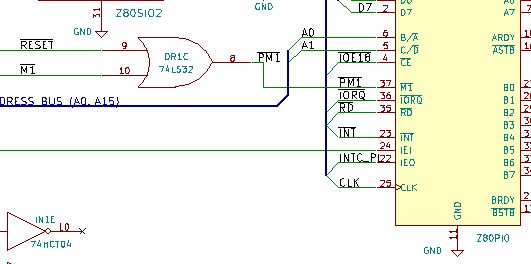
The "dependency effect" of using existing code also makes itself visible in hardware I/O address selection. To avoid changing too much code, it makes sense for me to place the SIO/2, ROM-disable and CF-disk I/O addresses on the same addresses used in Grant's design. I also liked his approach of using a 74LS138 for decoding, so I stuck with that approach, and selected "remaining" decode outputs for use with the CTC and PIO. The decoding logic ends up "eating up" 8 I/O addresses for each "on-board device", so 40 I/O addresses in the ranges 0x00 to 0x1F and 0x38 to 0x3F are locked. Somewhat expensive in terms of resources, but it allows for a simple construction with few parts. Besides, all addresses from 0x40 and up to 0xFF are still available for expansions.
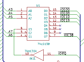
I/O address decoding for on-board devices
As listed, I wanted to be able to use software-controllable bit/baud rates on the serial ports. To be able to do that I chose to include the Z80CTC, a counter/timer controller, to drive the SIO. But I wasn't quite sure about my Z80 assembly skills yet, so I decided to include a jumper-selector to select SIO-clock to be CPU clock or CTC. That way, I could select CPU-clock for booting unmodified code from Grant, and then switch to CTC-clock once I knew how to do that.
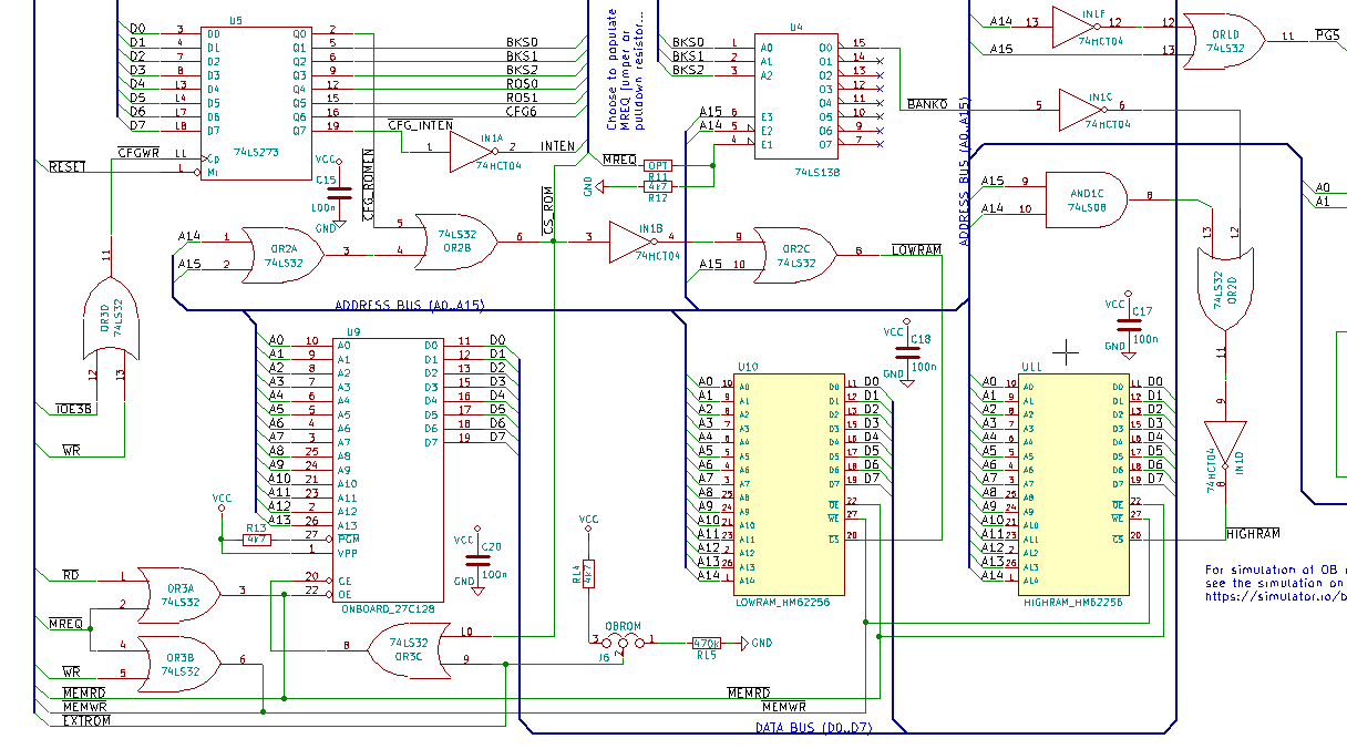
My first major divergence from the base design came as a result of my desire to have a memory map designed for graphics. Being able to combine that with the option of running code other people has made for Grant's design, meant that I had to include some kind of bank-switching. The design already included a very basic form of bank-switching: Grant has designed the "disable ROM" feature as a simple RS-latch that bank-switches the lower 16k between ROM and RAM. To switch from the ROM bank to the RAM bank, a write to address 0x38 needs to be done. In his design, the bank switch is triggered by an I/O write to the correct address, and the data is not used for anything. I examined the source code and found out that even if you only need to write something to the address, his code actually writes the value 0x01. Based on that, I decided that my "memory management" for bank-switching could be done using some kind of register, placed at 0x38, as long as the lowest bit of the register was used for enabling/disabling ROM. This would additionally give me the option of switching ROM back in, in contrast to Grants design where only a system reset would bring ROM back into active memory.
Armed with a general idea on how I could do bank-switching, I started looking at how I could make a memory map that worked with both CP/M and graphics. Because CP/M needs to have its BIOS and BDOS placed in a predictable, always available location in memory, and it expects RAM in the bottom of memory, my options were a bit limited. On top of that, I wanted to at least start with existing software, and the software I had available expected to be able to stuff BDOS, BIOS, ISRs and stack in the top 8-16k of memory. That made me decide to use a fairly odd and uncommon memory map. I decided that the second-top-most 16k would be the "window" for bank-switching. Basically, bottom 16k is switchable RAM/ROM, second 16k is always on-board RAM, third 16k is switchable memory defaulting to on-board RAM, and fourth and final 16k is always on-board RAM.

Memory map / layout for LiNC80
With the general memory map laid out, I turned my attention back to that register I talked about earlier. I decided I'd go for the simplest approach I could think of, one that I had used to implement a simple digital-out solution for the RC2014 computer. By using a 74LS273, I could get a very simple 8-bit write-only register. To quote the data sheet: «The SN54/74LS273 is a high-speed 8-Bit Register. The register consists of eight D-Type Flip-Flops with a Common Clock and an asynchronous active LOW Master Reset.». Placing one of those on I/O address 0x38, using IO Write as clock input and the data bus as D-inputs, I could use the outputs to perform bank switch selection. Using the system RESET signal for the '273s Master Reset, the system would always reset to a predictable state. And by using the lowest bit to control ROM disabling, I had compatibility with the existing code from Grant! With seven bits still available, I decided to use three bits for RAM bank select. This would let me simply use another LS138 to select one of eight RAM banks, and by using "location 000" for the on-board RAM, things should boot nicely.
I selected to use one bit of the "register" to control Interrupt Enable Input of onboard devices. This would let me "lock" interrupts to an IM2 disabled state, a feature I thought would be handy to have on top of the Interrupt Enable / Disable Interrupt instructions of the CPU. This left me with a few bits left over. In my scribbling, the idea of having a ROM cartridge for fun and experimentation had been added. I quickly added to that idea, by using two of the bits as "off-board ROM bank selects". That would allow a ROM cartridge to have four 16k banks! Which by the way matches nicely with a standard 64Kbyte ROM chip size.
With memory map idea fleshed out, I had to figure out a way to make the memory decode and interfacing work. I ended up finding a cool tool at https://simulator.io/ that allows for on-line simulation of digital logic. Using first a set of logic tables, I assembled an idea, and implemented it on simulator.io first, before adding it to my design. You can see and play with the result at https://simulator.io/board/RoLQ8QDEei/2. Confident that I had a memory layout that could work, and a decode logic that seemed to make sense, I started the actual design. The resulting memory interfacing logic took quite a bit more glue logic than Grants simple design, but I think it came out quite nice.
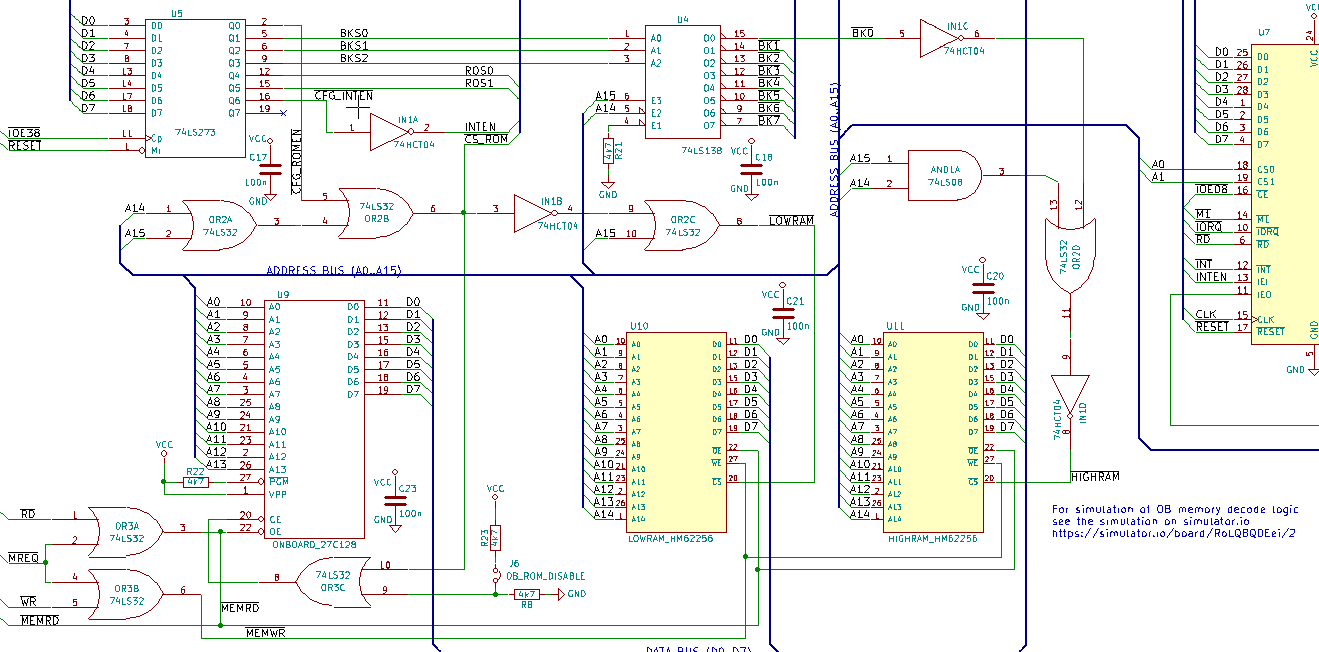
Memory logic Revision A of my Z80 design (with flaws)
The overall schematic I had in KiCAD was at this point starting to get large and complex. Thinking back at my issues with flaky breadboards, I was starting to dread building something as complex as this on either wonky breadboards, or on a very large perf-board. It would be doable, but the thought of debugging soldered point-to-point or bad breadboard connectors didn't really sound tempting. At the same time, I was still learning to use KiCAD for a somewhat large design, and I more or less accidentally started laying out a PCB. Combining manual parts layout, a bit of manual routing and experimentation with freerouting, I suddenly had a board layout that looked decent. So I took a gamble, and simply sent off some money and a few gerber files to seeed studio. Not a full week later, I received a box containing five fine looking PCBs.

This board was designed with all the bullet points from the design list. There's SIO/2, CTC and PIO devices, an IDE connector, and on the right side, a Z50Bus expansion bus. Additionally, I created a different version of an expansion connector on the left side that included all the decoded bank-switching lines (but not all CPU-signals, to keep it on a 50-pin connector).
Seeing how nice my PCB looked, I got to work assembling it. I soldered in passives, added sockets for IC's, and completed all soldering. After some experience with how much rosin flux can affect a complex logic circuit, I cleaned the board thoroughly before adding any of the semiconductor components. Finally, I hooked up serial ports and applied power.
Nothing happened.
Or, well, something happened. The board started drawing current, and it was well within expected range. So it would seem that the reason for it not working wasn't a dead short or a major defect. It had to be some kind of logic design flaw. I got a hold of a cheap logic analyzer to try to figure out what was wrong, but I couldn't get the analyzer to trig properly on the T1-T3 multi-clock-per-instruction that the Z80 has. I shelved the project in frustration for a while. After some months of not working on it, I brought it back out, and started poking around. After seeing some weird behavior, and a bit of "almost working" if I removed both the 'LS138 and the 'LS273, I figured something was weird with the I/O addressing. On examining the schematic in detail, I realized I had made two really silly mistakes.
The I/O address decoder was always active, doing its decoding even on Memory operations and even on the built-in DRAM refresh. Next, the 'LS273 that I was using as my "configuration register" only used the I/O address decode signal as its "Write" signal! These two problems together meant that the contents of the "register" was constantly changing. I'm not surprised that the code in ROM was less than happy about getting bank-switched out half-way through an instruction... Fortunately, I had spare logic elements in the glue logic IC's. This allowed me to fix the problems using bodge-wires and cut traces on the back of the PCB. The same evening I discovered my errors the system started doing what I had intended, and I had working CP/M on my slick-looking homebrew PCB.

I decided it would be best to fix the mistakes in my schematic, so I went back to KiCAD and implemented the changes that I had made on the board. I swapped some gate selection around to make the glue logic easier to route. While I was looking at the routing issues, I had a long think about the whole "two expansion ports, one for system and one for graphics". In the end, I decided it did not really make sense. I could put all the memory/bankswitch and graphics-only signals on a much smaller header connector, and use a cable to a standard Z50Bus expansion card. That would mean only one expansion connector would be needed. This in turn would lead to much simpler routing of the board, and the board could be physically smaller, reducing cost.
Reducing cost may sound weird. After all, this is my homebrew design, and I already had a working computer in front of me. But at this point, I was seriously considering making this a kit. And if I was to sell any of these, making the cost of the PCB go down would be a good plan. So, the changes were implemented, I did a new layout, and sent it off to seeed for fabrication. 10 days later I got a new batch of boards that I fairly quickly assembled. I transplanted all ICs from the previous build over, and tested it.
And it did not work. ARGH!
Back to the schematic, I found ONE silly mistake. While I was redesigning, I had done some changes to the schematic around the SIO/2 chip, and while doing that, I had swapped the address lines A0 and A1 by accident. That meant that the Control and Data addresses had become swapped. A quick cut-and-solder on the PCB swapped those back, and the computer came to life! I set to work writing code to test the other on-board devices that aren't on Grants design. I got the CTC to clock and generate interrupts, and I got the PIO to work as Byte-out, Byte-in, and bit-in-out. But no matter what I did, I could not get the PIO to generate interrupts.
It turns out, the PIO interrupt signal is gated by its M1 input. And, because the PIO actually has one pin less than it needs, Zilog chose to make a multiplexed M1+Reset function on the M1 pin. And in my design, I had thought "M1 input is active if either CPU M1 is active OR if system Reset is active". So I had put an OR gate there. There's one problem with this. Both Reset and M1 are ACTIVE LOW signals. And to make an "or" function for active low signals, you need to use an "and" gate! Long live boolean logic and active low signals. Who would have thought OR to be different from AND in boolean logic... I managed to finagle this by more bodging, and eventually I had a fully working computer, where all on-board devices worked.
Considering the amount of self-inflicted troubles I had experienced so far, I decided to test the expansion bus and the ROM cartridge connections before fixing my schematic again. To my relief, both of those worked without problems. I was able to use a ROM cartridge with ROM bank select, and was even able to use the RC2014 backplane to test using off-board memory and off-board devices.
During the testing of the ROM cartridge solution, I discovered that the rule of only using parts still in production had been violated on my design. I had based the on-board ROM circuit on a 16Kx8 EPROM, the 27c128. That ROM chip is not available, and neither is it's EEPROM-version, the 28c128. Fortunately for me, the bigger AT28C256 is still in production, and very close to pin compatible. I revised the schematic and board to include two jumpers for on-board ROM allowing either tied VCC signal for 'c128-devices, or use of the ROM-select lines. This makes it possible to select between 'c128, 'c256 and 'c512 ROM chips (16k, 32k and 64k), and even use of bank switching for on-board ROM. The physical placement of the jumpers was done so a ZIF-socket would fit (it's tight, but it fits), just because I could.

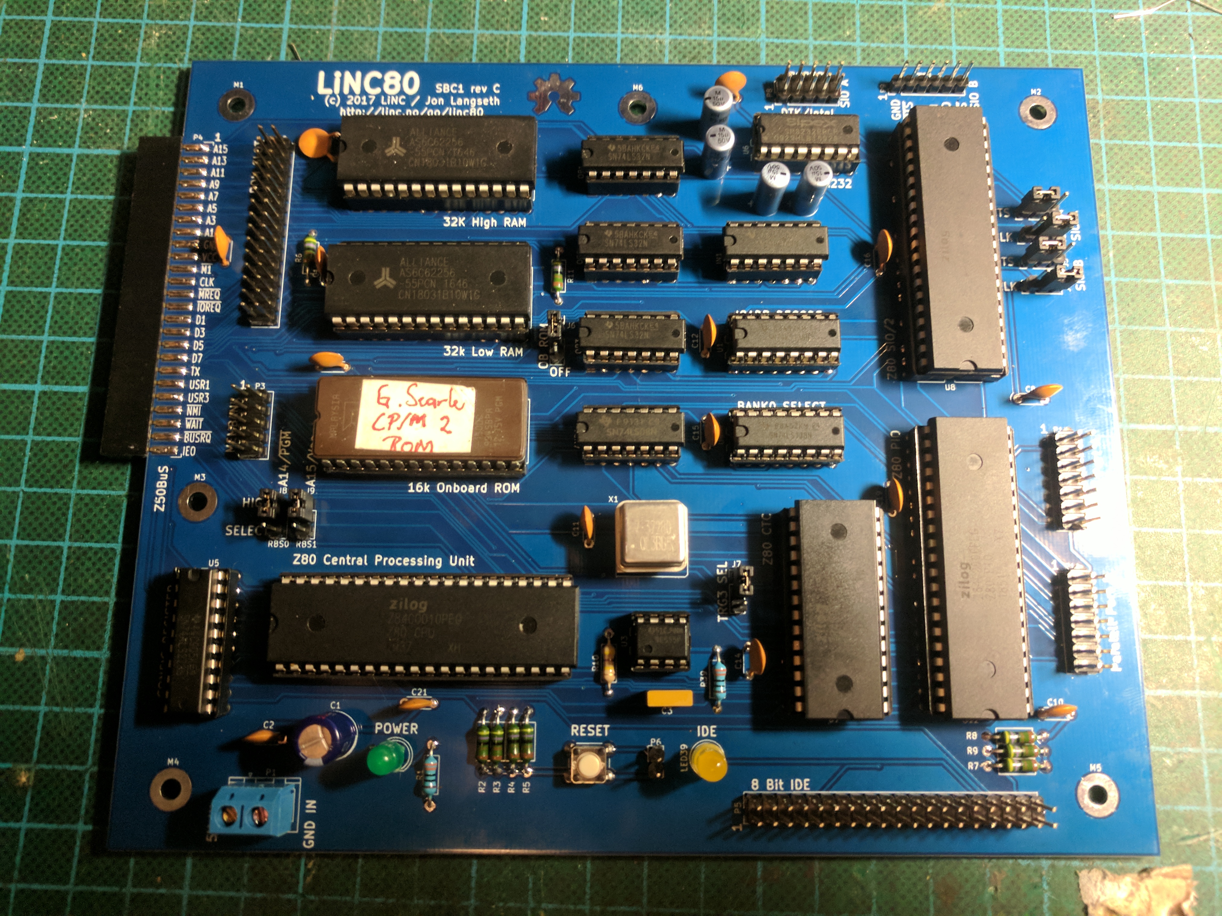
Considering the errors in this revision B of the board, I made corrections, and created revision C. This board now carries my official name for my homebrew computer design as it stands today: the LiNC80 Single Board Computer 1 Rev C. Considering it is an expandable board, with no on-board graphics, it may seem strange that I call it an SBC. Before the arrival of a heap of BeagleBoard and Raspberry Pi like devices, it was usual to call a PCB that implemented a fully working embeddable computer an SBC, and it was unusual for SBCs to have local graphics, but not unusual for them to have expansion/interface connectors.
Revision C of the board still has a minor issue, but none that makes a real difference to a system user that is aware of it. The only significant problem I see at the moment, is related to how the two serial ports behave on RTS/CTS signals if one of the ports is left unconnected. On the board, there is a jumper that selects between honoring incoming CTS (RTS from other host), or tying it to Gnd. If unconnected and not tied to Gnd, the SIOA tends to lock up the second serial port SIOB. On the other hand, if SIOA is connected, but SIOB is left unconnected, random characters may get generated if the CTS input is floating. The solution is to jumper the unused CTS signal to "disabled" for an unconnected SIO port.
This post is part of a series documenting my journey in making my own homebrew computer, the posts can be found on this link. Stay tuned for more posts in this series. The next will probably be about the various adapter cards I have planned/made.
Note! I am gearing toward making kits available!
The product description pages for the kit starts off at http://linc.no/products/linc80-sbc1/
The new, more official page for the Z50Bus is located at http://linc.no/products/z50bus
Building a CP/M compatible system on perf-board
With a fresh success of building a computer from a kit, I decided to implement an existing design on perfboard, instead of drawing a design of my own right-away for breadboard building. Considering that the RC2014 is closely based on the work of Grant Searle, it was natural for me to take another design of his, and adapt to the 8-slot backplane: the "fully functional CP/M machine using only 9 chips" design.
I broke the design down to separate functional blocks, and built each as a separate card. By splitting the build into these distinct parts, I was able to build one card, and verify functionality of that card using the RC2014 before continuing to the next. All the cards were built on 100mm wide perfboard, using a direct soldered wire approach.
- RAM/ROM card
- SIO/2 serial IO card
- 8-bit IDE adapter for CF card
- CPU board with onboard Clock and Reset
- YM2149F sound card
I chose to make the RAM/ROM as a single combined card, because I did not want to split the ROM-disable function needed for CP/M up across two cards. It also allowed me to reduce the potential part count (by 1 IC). Because of the close relationship between the RC2014 design and the one I was implementing, I could simply use the ROM content from the RC2014 for verifying the ROM/RAM using the CPU and Serial I/O board from the kit.

Point-to-point wire soldered RAM/ROM card
Grant's CP/M design uses a different UART from the BASIC design. The BASIC design uses a 65B50, while the CP/M design uses a SIO/2. So this was the next card to be built. To verify this one, I burned a new ROM containing the "monitor" for the complete CP/M-design. This monitor also includes an 8k BASIC version, so it was easy to verify the SIO/2 board without having a CF-storage approach available.

Digital Out, RAM/ROM and SIO/2 cards installed
The original breadboard design page talks a bit about how to wire up a Compact Flash card, and how to hand-solder the SMD connector used for CF-cards. I did really not want to deal with that connector directly, and gambled on being able to use an IDE-to-CF adapter, considering the design really uses CF in 8-bit IDE mode anyway. My "IDE adapter" is basically a couple of OR-gates, an '138 address decoder, some resistors and a 40-pin male header connector. And it worked! With a short IDE cable between my "adapter" and a commercial IDECF-adapter, I was able to prep the CF card, load software onto it, and boot to a lovely "A>" prompt!

Possibly the simplest IDE adapter I could make
I could have rested here, but decided to whip up a new CPU board, as that, plus the clock generator, now was the only cards from the RC2014 kit that was in use. I integrated the clock, and also added an auto-reset onto the CPU card.
With these cards on the backplane, I now had a working Z80 based system, that I had needed to do some desgin-work for myself to adapt it to multiple cards. It was even a working CP/M system, with bonus ROM-based BASIC. To further verify that I did indeed have a CP/M compatible system, I grabbed a copy of Zork 1, I think it was from http://www.retroarchive.org/cpm/games/games.htm, and loaded it onto the CF-card using Grant's DOWNLOAD.COM utility. I believe any fully CP/M compatible system should have a copy of Zork 1 on it. And mine does, and it works 😀 I have used Zork as a demonstration of the system so much now, that my friends and colleagues have started to call my homebrew CP/M computers "the Zork machines" 😀
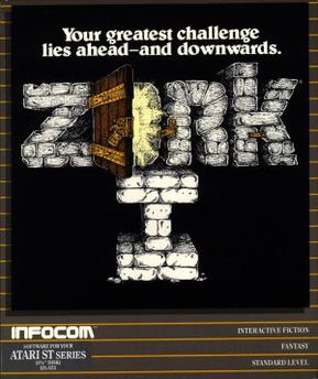
Zork I box art
The final card I built for the RC2014 bus, was a YM2149F synthesizer sound chip adapter. It required some fairly weird address decoding logic, so I spent quite a while on the design of this relatively simple card. After laying it out on perfboard and soldering up the wiring, I had a working sound card. I do believe I am starting to get a hang of this... What I still don't have as good a hang of, is large-scale assembly projects. So, I have tested the YM-card extensively from BASIC, and I have some general test-routines for it written in Assembly. But I have not made any proper songs using it, and I am quite far from implementing a Tracker or Player of any kind.
What I have used the system for, however, is getting to know how to code z80 Assembly for CP/M. It's a neat little operating system. A task as "small" as reading a file from disk has you digging quite deep into the system itself. As a result you end up with a very deep understanding of how the operating system internals work. And being such a small operating system, it is quite possible for a person to understand the entire operating system, after a reasonably short time studying it.
I created a final board for the system. By using a very cheap Chinese strip-board, I created a barebones version of the backplane. This freed up the RC2014 backplane to go back to being used with the original kit, and also made the computer a completely homebrew build. After this, the electronics part of the perfboard project was done. With such great results on the electronics side, I figured it deserved a nice place to live, and not become yet another stack of project parts in one of my bins of such. So I built a wooden cabinet for it, with some 3D printed parts to hold the cards in place. The case is made from beech wood, with an inlaid aluminium front.

My RC2014-based CP/M computer in a nice wooden case
This post is part of a series documenting my journey in making my own homebrew computer, the posts can be found on this link.
My first working homebrew was a kit: RC2014
After having solved the mystery of counterfeit parts, I felt ready to start attacking my master plan of building my own Z80 based computer. I wired up a CPU test circuit and used with great success. I then wired up a simple system on a set of cheap breadboards, consisting of the CPU, a ROM chip and a slow clock generator. With LEDs on the address bus, I punched up some simple assembly that NOP'ed for a while, did a JMP, NOP'ed some more, and then JMP'ed back to start. This was assembled using TASM under Dosbox, and loaded into the ROM using my Minipro programmer. When I applied power to the circuit, it started ticking along, and did just what I expected it to do!
Success! With great spirit, I next wired up a far more "complex" circuit. I added a few support logic gates, a 74LS138 4-to-8 decoder and a 74LS373 8-bit latch, and moved the LEDs from the address bus to the outputs of the latch. With the added components, I had a kind-of 8-bit digital output. With a simple counter code typed and assembled, I had partial success. The circuit and code worked. And then sometimes it didn't. And sometimes when it didn't work, it would start working after some time.

Breadboarded system with "Output port"
With the bad experiences from fake chips, I started suspecting that my cheap breadboards were causing problems. So I moved the circuit over to one of my "known good" breadboards, part of an old digital trainer device. Now the circuit and code worked most of the time, but still sometimes not. I was getting frustrated. I tore down my wiring, checked and verified my circuit, wired it back up, and got the same result. Was there something that I had completely misunderstood? Was there something very wrong with my method?
Eventually, I decided to stop faffing about. I decided that the best way forward, would be to start building a known good design. With that, I would be able to verify that I am able to pull this off, and I would be able to use it to test and verify what I was designing from scratch. So, enter the RC2014!
It was now late december 2015, perfect timing for a "christmas gift to self" kind of a purchase. In my research for options and ideas, I had looked at Spencer Owen's RC2014 several times. It is a dead simple design, and cheap as well. Perfect match. Off to Tindie I went, my order placed on saturday the 19. december. I was very impressed when the kit arrived in my mailbox on the 23rd! I brought the kit with my on my Christmas holiday, and by the 27th it was completed. I connected up a TTL-USB adapter, and powered the thing up. To much joy, the kit sprung to life! Grant Searle's BASIC monitor greeted me with Microsoft BASIC for Nascom (modified by Searle and Owen).

WorkingRC2014, running example colour fractal code
This was back when the only RC2014 kit available was the "Classic" version. My kit was the "Full monty" set, with all components, and the 8-slot backplane. The kit was genuinely well put together. The PCB's are simple, but cleanly presented. Components were well packaged, and sorted. The instructions were simple, but clear and concise. The overall packaging was small! As for ease-of-build, there are many connections to solder, and get right in a kit of this type, so I would not recommend it to a beginner. But even with the simple pen-style soldering iron I keep at mum's home, I was able to complete the job cleanly in a reasonable amount of time. So I'd call it an intermediate kit easily. I can happily recommend Spencer's kits, and the new, updated versions of RC2014 kits look nice indeed. I'm tempted to buy another one, to be honest 🙂

RC2014 kit contents
I now had my first working Z80 based homebrew computer! And with an 8-slot backplane, I had 3 slots available, as the original kit uses 5 slots: CPU, ROM, RAM, Serial I/O and Clock generator. With a simple bus format using Single row connectors, it should be easy to make expansion cards. I dug out a perf-board, added the needed right-angle single-row header pins, and soldered up the exact circuit I had tried on my breadboard. I plugged it into the backplane, and tested it using OUT statements in BASIC. It worked! Another great success, but at the same time somewhat of a mystery to me. Why did it not work on breadboard, when it worked fine in a more complex system? I decided to test removing the RAM and Serial cards, and load my test-ROM onto the ROM card. Suddenly, the I/O board was behaving erratically again. Thanks to RC2014, I now had proof that my hardware was working, and my software was bad. The kit had actually already accomplished what I wanted: verify that I could assemble a working system from someone else's design, and verify that I could design working hardware myself.

Working homebrew 8-bit output card on a complete RC2014 system
All of this made me make a change of plans. Instead of going back to the breadboard, I decided to try to implement Grant Searle's Minimal CP/M system using home-built cards for the RC2014 backplane, before proceeding with my own design. The process of this is the topic of a post of it's own.
I have since (much later, really) dug out the wonky test-code, and corrected my mistakes. I can't remember what exactly was wrong, but I seem to remember it was embarrassing. I have not tried wiring it up on breadboard again, as all my Z80 CPUs have been busy running on other systems 🙂
This post is part of a series documenting my journey in making my own homebrew computer, the posts can be found on this link.
Scribbling ideas for a homebrew computer design
This is part two of a series, documenting my journey in making my own homebrew computer (previous post here). As the title suggests, it looks at my process of selecting a design. But first, as I am a computer history nerd, a little computer history ...
The world of computing as we know it wasn't in my opinion started by the big behemoths of the early computing age. Yes, they created the field of computing, and through steady capability increase combined with reduced sizes made the systems we have today possible. But it required the invention of the microprocessor to make the idea of personal computing a realistic idea. Before that, it seemed computers was something for big businesses, universities and research institutes. But with the creation of chips, originally designed for flight computers in jetfighters and for calculators at accountant desks, hobbyists started playing with the idea of creating a computer of their own! Early on, the homebrew computer systems was the way to get a computer in a private home. Early examples of commercial personal computers, like the Altair 8800 and Processor Technology Sol-20 were in reality business-backed homebrew systems. In fact, the first of these commercial systems were shipped as blank PCBs and bags of components. Even the famous Apple I computer is an example of this. It is this enabling of computers in the average Joe's hands that enabled the explosion of computing that has lead to the technology enabling we have today.
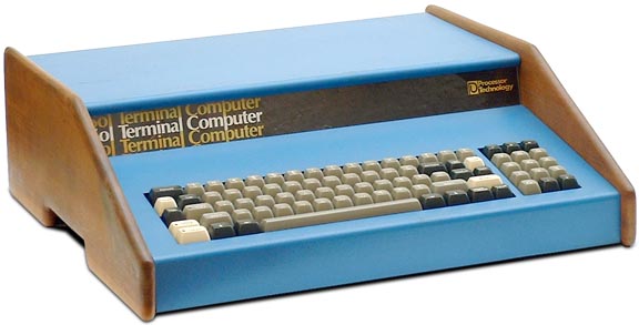
Sol Terminal Computer / Sol-20
So, to design thoughts and ideas. I wanted to create a computer that fits in the era of homebrew. This means to me, a fairly low-end system, designed by an individual or a small group of people, using time-period components, to be built in the home. If my design is able to be produced as a kit, that fits right in with the "standard" of the day. System designs were prototyped in basements and cellars, to later be sold as kits for other people to brew at home, and modify and expand. It was natural for me to select an 8-bit platform as my target, after all the 8-bit "revolution" was at the core of homebrew. As mentioned, I wanted to use time-period components, but I also wanted to be able to create my system without having to resort to "New-old-stock" or cannibalizing of parts to get a hold of parts that are no longer manufactured. This put some hefty restrictions on my options, and also meant I had to allow myself to use a few bits of "modern" technology.
This brings me directly to the choice of a CPU for my system. I talked about how the 6502 was the first CPU that I got to know in-depth in my previous post. Unfortunately (or fortunately, take a pick), I early on decided that the 6502 would not be the CPU for my system. While the CPU is still available, in a CMOS-ified version with added instructions (W65C02S6TPG-14), it would require some supporting components that are no longer available (other than NOS) to make a full computer that I would be happy with. With that realization, I started looking at what other microprocessors were used in significant number of designs. Candidates seemed to be: RCA CDP1802, Motorola 6800, Intel 8088, Intel 8086 and Zilog Z80. Of those, the only one that has an active, still in production version that's not a derivation is the Z80. As a bonus for choosing that one, it comes in a bread- and perf-board friendly 40Pin DIP, and has significantly simpler interfacing than the other options, by having full address- and databuses, simple single-phase clock and a trivial voltage-supply requirement of simply 5Volt. The Z80 was also designed to be relatively compatible with the 8080, so a lot of existing software runs on both CPUs.
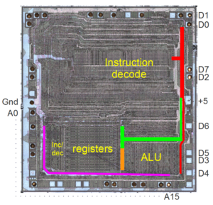
Annotated photo of Z80 die, by Ken Shirriff
Landing on the Z80 gave me additional things to explore. Being a retrocomputing-nerd, I have for a long time wanted a system that could run CP/M. Control Program for Microcomputers is a very significant part of Personal Computing History, and a great number of systems, both commercial and homebrew, either had CP/M ported, or were designed specifically for it. With the Altair and IMSAI computers kick-starting a form of standardization with the S100 bus, CP/M became more or less the standard operating system for general personal computers, and thus had a majority share of the system software marked. It was only beat by the multitudes of different ROM BASIC versions summed up. CP/M was designed for select 8-bit Intel 8080 development systems, but due to its design it was easily ported to compatible machines, and with the compatibility of the Z80, quite a lot of systems were designed with just that CPU. While exploring what it would take to let me design a CP/M friendly system, I discovered Grant Searle's brilliant set of designs. On taking in the content of his site, I was first impressed by the amount and quality of work mr Searle has done to make his systems available and understandable. Second, I was blown away by how simple a CP/M system could be. So my path was early on set; I would take inspiration from those designs, and get CP/M running!
With a path staked, my plan became to try implementing the "Fully functional Z80 CP/M machine using only 9 chips" from Grant Searle on a breadboard or perfboard before proceeding to attempt a design of my own, to make sure that my understanding of the complexities involved was sane. However, I allowed myself to start sketching ideas for what I wanted to accomplish with my own design while waiting for parts. The journey of trying to get the first system operational will be documented in separate articles, this one is about the sketching...
My homebrew hybrid prototype of Grant Searle and Spencer Owens's designs
One of my early design choices was between simplicity or expandability. I had looked at the designs in the Retrobrew Computers community, and generally thought they were trying to be somewhat more "modern" than what I was trying to achieve. I wanted something that was a bit simpler, but at the same time I thought that having the option of extending the system would be great. This led to quite a few nights reading up on various bus architectures from the homebrew era, thinking about using one of the "standard" options like S100[1][2] or STD80[1][2]. One big issue with using one of the full-featured old standard bus designs was that it would require a lot more complexity than I wanted. So I decided not to go down that route, and rather go for a more raw CPU signal extension bus.
While examining what I would need to put on such an expansion interface, I became aware of Spencer Owen's RC2014. His first version of the RC2014 was basically Grant Searle's simple Z80 BASIC system, split into multiple cards, one for each major component, connected to each other on a simple 40-pin perfboard-friendly bus-approach. I really liked the concept, but saw a few challenges in it. It used single-row 2.54mm spaced header pins, and omitted a few signals that I knew would be needed later. From experience, I felt that using double-row connectors would lead to more solid mechanical properties, as well as making the bus mechanically smaller. Spencer's bus does not "fit" on a 100mm wide PCB, a real issue as prices for PCBs (and EDA/CAD if not using KiCAD or EasyEDA) has a definite crossing point at exactly 100mm... A double-row physical layout would also very easily translate into a card-edge implementation if one would like a truly retro feel... There will be a (possibly short) article about the result, with pinout and concept released to the public domain. I call my idea/approach the Z50Bus.
With a bus inspired by RC2014, it would also be possible to take advantage of the many cool designs that Scott M Baker has made. Take a look at http://www.smbaker.com/category/electronics-projects/, he has some really sleek additions and extensions based on the fairly simple RC2014. After seeing what smbaker has been able to do, I was sure that I wanted a simple, yet complete CPU bus, and that way be able to reduce the amount of "onboard" features.
Originally, I really really wanted to have a graphics system as a direct part of my design. Quite a lot of time was spent thinking about using memory-mapped or register/io-space based with their pros and cons, debating using a prefab Video Display Processor like the VIC, VDP or Yamaha V-series, and researching indexed video, colour-register based approaches and planar graphics. After seeing FAP, the FPGA Assisted Processor, I came to the conclusion that using an FPGA would be very similar to the time-period correct ULA, PLA and CPLD approaches that were actually used on Home Computers of the 1979-1985 period, just faster and reconfigurable. Going that route should allow a core hardware design to implement many different graphics subsystems, allowing experimentation.
However, I have chosen to not implement the actual graphics system initially! Most homebrew computers of the early microprocessor age didn't actually have graphics capabilities. Most didn't even support a keyboard. Generally the approach in the early days of homebrew computing was to use a teletype terminal, or a video display terminal. So I decided, if a set of serial ports was enough to get the homebrew computing started, a set of serial ports would be enough to get my system started as well! After all, I had already included an expansion interface, so adding graphics and keyboard I/O later on would simply be just that; an expansion. However, to be able to use memory-mapped video later, I would have to design my memory-map and RAM-interfacing with that in mind. The memory map, and the reasoning behind it is topic for a separate article.
Similar to the decision design for graphics as an expansion, I decided that storage media like floppy disk support is to be an expansion. I intend to create a floppy disk interface, for an actual floppy drive and/or a Lotharek HXC. Also on the roadmap is trying to go real retro, with a cassette interface. But I changed my mind about one form of storage connection. Even if IDE appeared on the market late in the 80's, it is too embarrassingly trivial to implement the 8bit microcomputer compatible mode of IDE. With a sane I/O interface like the Z80 has, all that is required to get working 8-bit mode IDE is a simple address selector, and two OR-gates and a few resistors. Plop a Compact Flash card adapter onto that, and you have an interface to solid state storage "for free". The fact that Grant Searle's CP/M computer uses that exact approach meant that is was an obvious choice for me to include it.

Hand-drawn early version of the system design
So, my basic design was centered around a Z80 CPU, with a memory map that would work with CP/M and a future graphics expansion, and serial ports for console and communication. To make it possible to have reconfigurable serial port speeds, and also general purpose timer triggered events I figured I needed to include some form of timer controller as an on-board peripheral. It would also be nice if interfacing with the "outside world" was easy, so adding one or more configurable parallel I/O ports made sense. The more I looked at that spec, the more obvious it became that I was more or less describing the standard Zilog "stack" (minus the DMAC): Z80 CPU as the processor, Z80 SIO for serial ports, Z80 CTC for the timer/counters and the Z80 PIO for two parallel ports. From this, it became natural to also design the system to take full advantage of the somewhat special, but cool Z80 Interrupt Mode 2.
IM2 is designed with a very powerful daisy-chain form of interrupt priority and arbitration. In IM2, devices are daisy-chained using their Interrupt Enable In (IEI) and Interrupt Enable Out (IEO) pins, with priority being resolved by their order in the chain. Additionally, interrupt handling is vectored, with the CPU providing upper 8 bits and the interrupting device providing the lower 8 bits of the relevant Interrupt Service Routine to be executed. The whole IM2 system looked very nice to me, so it is a central design element. It introduces challenges when trying to use non-Zilog peripherals unfortunately, but Luke Maurits has given me some ideas to solve that later from his LM-512 Homebrew computer.
As part of my process of building my "learning computers", in the forms of Grant Searle's CP/M computer and Spencer Owen's RC2014, I figured that following an approach close to those made sense. Using 74LS138 for address decoding of on-board peripherals was a safe and natural approach. To enable a memory map for CP/M plus expansion for graphics, I decided to add a "write-only configuration register" by including a 74LS273, placed at the IO address that Grant's monitor ROM uses to enable/disable onboard ROM. I decided that I did not want the complexity of catering for a large memory space, onboard memory was set to 64kbyte onboard RAM, 16k onboard ROM, with a bit of banking for a max configuration of 176k ( 16k*8+48k) RAM and 64k (16k*4) ROM in an expanded system using memory banking via the configuration register. This configuration would allow use of CP/M, expansion with graphics and storage later, but it restricts the system to not be compatible with Fuzix by Alan Cox et al.
To close off a by now rather lengthy post, a summary of design conclusions is in place
- Z80 CPU
- Zilog SIO/2 serial port controller with dual serial ports
- Zilog CTC for four channels of Counter/Timer, 2 of them dedicated to the SIO/2
- Zilog PIO for two Parallel ports
- Expandable system through Z50Bus
- Memory map designed to allow for graphics expansion
- CP/M compatibility
- ROM part of memory from address $0000 disable-able (needed for CP/M and more)
- For fun, a dedicated ROM Cartridge connector
- Z80 Interrupt Mode 2 in the core
- Compatibility with software from Grant Searle (for easy system bring-up)
The last point in the list turned out to be very useful, as it allowed me to tackle a bunch of problems I encountered, without having to also write my own system ROM monitor. It also let me simply load up CP/M onto a CF card and start playing Zork!
Nostaliga: Emma II and the desire to make a computer
This article starts a series, documenting my journey in making my own homebrew computer.
Back in ye olde times of 1994 I attended vocational secondary school as a student of electronics, and during that time, I was introduced to the wonderful lady Emma II. Emma was a "trainer" system based on the MOS Technologies 6502 CPU, in many ways related to the somewhat more commonly known KIM demonstration and development system. This sparked a love for quirky 8-bit computer systems that's still with me today.
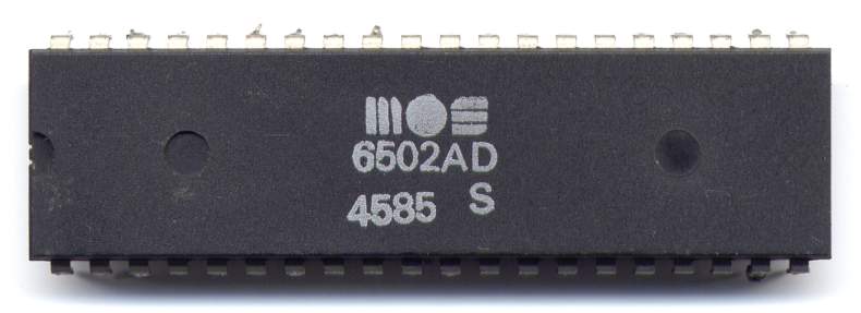
MOS 6502 CPU, image CC BY-SA Dirk Oppelt / Wikipedia
http://retro.hansotten.nl/6502-sbc/emma-by-l-j-technical-systems/
http://www.anf.nildram.co.uk/beebcontrol/arms/atlas/emma.html
Using Emma's (fairly flakey) hexadecimal keyboard, we were set to program the 6502 using opcodes and raw data bytes. To solve the task, we had to design our programs using flow charts drawn on paper, and then translate the flowcharts to pseudo-code. With an idea of what the programming should look like, we sat down studying the manuals for the 6502 CPU internal structure, how it operated, and what it's view of memory and the world looked like. Next the manual for the Emma II was examined in detail, to learn how what we now knew about the CPU was used to implement a full single board computer.[1][2][3][4]
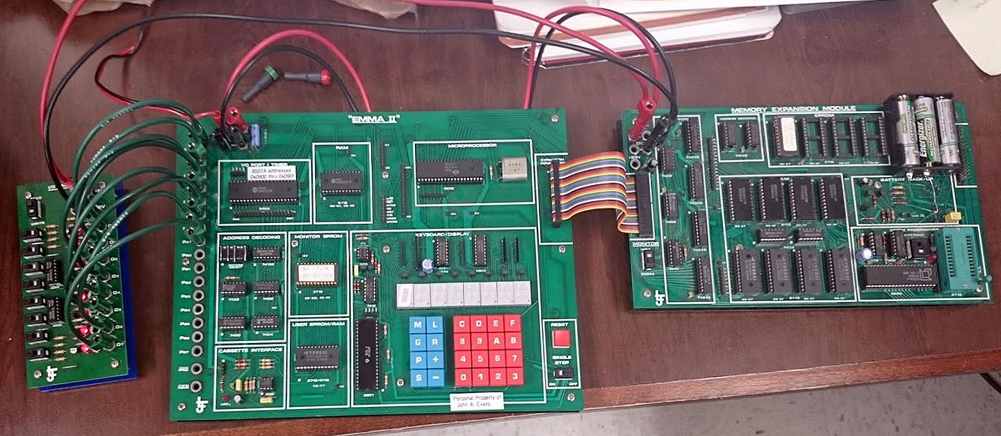
The 6502 trainer Emma II by LJ Electronics. CC BY-NC-SA Hans Otten (http://retro.hansotten.nl)
Armed with oodles of new information, our next task was to transform our flow-charts and pseudo-code into something Emma could understand. And that meant hand-translating our concept, first into Assembly mnemonics, and next to "hand-compile" our ASM-code into 6502 opcodes. The joy when our "traffic light simulator" finally worked! The frustration when our "lift controller" never worked... The satisfaction of coding up a lottery-number-picker of our own design, and having it work on the second try! Details such as zero-page, indirect and immediate addressing and the importance of understand addressing modes are still (if somewhat ratteling) stuck in my head 🙂 And I will easily claim that the experience of having to opcode-program a computer system has given a solid foundation for my later work and understanding in the field of information tech.
Even if we (naturally) were using more modern and advanced computer systems for our day-to-day tasks, and the Internet was about to explode (actually, my 2nd-year project in spring of 1995 was internet-enabling the school), the raw nature of the 8-bit computers fascinated me, and the simplicity of such a system had me thinking "This is something I can design and build from".
Alas, I had to leave Emma at school. But a short time later, I came in possession of two 6502 CPU chips, an 8086, a weird thing named 80186, and also an even weirder named thing called a Zilog Z80. These parts rattled about in my parts bin, and my head for many long years. My hope, and intention, was to build a computer from at least one of these. A fairly simple 8 bit system, with RAM, ROM and some form of communication on a higher level than the sponge-like flaky keys of Emma was the whole "design".
I am happy and proud to tell that I have now completed that task! In a series of articles, I will tell about the 2-year journey that lead to a fully functioning 8-bit computer, not at all built on the 6502 🙂